JAJSJN3B december 2020 – july 2023 BQ25672
PRODUCTION DATA
- 1
- 1 特長
- 2 アプリケーション
- 3 概要
- 4 Revision History
- 5 概要 (続き)
- 6 Pin Configuration and Functions
- 7 Specifications
-
8 Detailed Description
- 8.1 Overview
- 8.2 Functional Block Diagram
- 8.3
Feature Description
- 8.3.1 Device Power-On-Reset
- 8.3.2 PROG Pin Configuration
- 8.3.3 Device Power Up from Battery without Input Source
- 8.3.4 Device Power Up from Input Source
- 8.3.5 Dual-Input Power Mux
- 8.3.6 Buck Converter Operation
- 8.3.7 USB On-The-Go (OTG)
- 8.3.8 Power Path Management
- 8.3.9 Battery Charging Management
- 8.3.10 Integrated 16-Bit ADC for Monitoring
- 8.3.11 Status Outputs ( STAT, and INT)
- 8.3.12 Ship FET Control
- 8.3.13
Protections
- 8.3.13.1
Voltage and Current Monitoring
- 8.3.13.1.1 VAC Over-voltage Protection (VAC_OVP)
- 8.3.13.1.2 VBUS Over-voltage Protection (VBUS_OVP)
- 8.3.13.1.3 VBUS Under-voltage Protection (POORSRC)
- 8.3.13.1.4 System Over-voltage Protection (VSYS_OVP)
- 8.3.13.1.5 System Short Protection (VSYS_SHORT)
- 8.3.13.1.6 Battery Over-voltage Protection (VBAT_OVP)
- 8.3.13.1.7 Battery Over-current Protection (IBAT_OCP)
- 8.3.13.1.8 Input Over-current Protection (IBUS_OCP)
- 8.3.13.1.9 OTG Over-voltage Protection (OTG_OVP)
- 8.3.13.1.10 OTG Under-voltage Protection (OTG_UVP)
- 8.3.13.2 Thermal Regulation and Thermal Shutdown
- 8.3.13.1
Voltage and Current Monitoring
- 8.3.14 Serial Interface
- 8.4 Device Functional Modes
- 8.5 Register Map
- 9 Application and Implementation
- 10Power Supply Recommendations
- 11Layout
- 12Device and Documentation Support
- 13Mechanical, Packaging, and Orderable Information
9.2 Typical Application
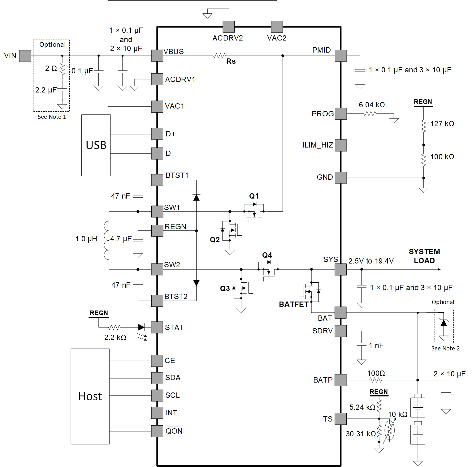
 Figure 9-1 BQ25672 Application Diagram
with Two Input Sources and Ship FET
Figure 9-1 BQ25672 Application Diagram
with Two Input Sources and Ship FET- Recommended if hot plugging adapters > 15 V.
- Recommended if hot plugging 4S battery packs with long leads or PCB traces.
 Figure 9-2 BQ25672 Application Diagram
with Single Input Source and No Ship FET
Figure 9-2 BQ25672 Application Diagram
with Single Input Source and No Ship FET- Recommended if hot plugging adapters > 15 V.
- Recommended if hot plugging 4S battery packs with long leads or PCB traces.