JAJSMK1 August 2023 BQ25756
PRODUCTION DATA
- 1
- 1 特長
- 2 アプリケーション
- 3 概要
- 4 Revision History
- 5 概要 (続き)
- 6 Pin Configuration and Functions
- 7 Specifications
-
8 Detailed Description
- 8.1 Overview
- 8.2 Functional Block Diagram
- 8.3
Feature Description
- 8.3.1 Device Power-On-Reset
- 8.3.2 Device Power-Up From Battery Without Input Source
- 8.3.3 Device Power Up from Input Source
- 8.3.4 Battery Charging Management
- 8.3.5 Power Management
- 8.3.6 Reverse Mode Power Direction
- 8.3.7 Integrated 16-Bit ADC for Monitoring
- 8.3.8 Status Outputs (PG, STAT1, STAT2, and INT)
- 8.3.9
Protections
- 8.3.9.1
Voltage and Current Monitoring
- 8.3.9.1.1 VAC Over-voltage Protection (VAC_OVP)
- 8.3.9.1.2 VAC Under-voltage Protection (VAC_UVP)
- 8.3.9.1.3 Battery Over-voltage Protection (BAT_OVP)
- 8.3.9.1.4 Battery Over-current Protection (BAT_OCP)
- 8.3.9.1.5 Reverse Mode Over-voltage Protection (REV_OVP)
- 8.3.9.1.6 Reverse Mode Under-voltage Protection (REV_UVP)
- 8.3.9.1.7 DRV_SUP Under-voltage and Over-voltage Protection (DRV_OKZ)
- 8.3.9.1.8 REGN Under-voltage Protection (REGN_OKZ)
- 8.3.9.2 Thermal Shutdown (TSHUT)
- 8.3.9.1
Voltage and Current Monitoring
- 8.3.10 Serial Interface
- 8.4 Device Functional Modes
- 8.5 BQ25756 Registers
-
9 Application and Implementation
- 9.1 Application Information
- 9.2
Typical Applications
- 9.2.1
Typical Application
- 9.2.1.1 Design Requirements
- 9.2.1.2
Detailed Design Procedure
- 9.2.1.2.1 ACUV / ACOV Input Voltage Operating Window Programming
- 9.2.1.2.2 Charge Voltage Selection
- 9.2.1.2.3 Switching Frequency Selection
- 9.2.1.2.4 Inductor Selection
- 9.2.1.2.5 Input (VAC) Capacitor
- 9.2.1.2.6 Output (VBAT) Capacitor
- 9.2.1.2.7 Sense Resistor (RAC_SNS and RBAT_SNS) and Current Programming
- 9.2.1.2.8 Power MOSFETs Selection
- 9.2.1.2.9 Converter Fast Transient Response
- 9.2.1.3 Application Curves
- 9.2.2 Typical Application (USB-PD EPR Configuration)
- 9.2.1
Typical Application
- 10Power Supply Recommendations
- 11Layout
- 12Device and Documentation Support
- 13Mechanical, Packaging, and Orderable Information
8.3.5.1.2.1 Max Power Point Tracking (MPPT) for Solar PV Panel
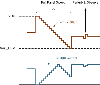
When EN_MPPT bit is 1, the device provides a maximum power point tracking (MPPT) algorithm for solar PV panel input sources. The Input Power Maximizer algorithm finds and tracks the maximum power point by alternating between full panel sweep and perturb and observe modes of operation.
The full panel sweep is used to find the input operating voltage which delivers the maximum charge current to the battery. Before running a full panel sweep, the device momentarily enters HIZ mode to measure input source open-circuit voltage (VOC). The device proceeds to reduce the input voltage regulation target, measuring the charge current output at each setting. The VAC_DPM register is used to program the minimum voltage to exit the full panel sweep. After the sweep is complete, the device updates the VAC_MPP register to the input voltage regulation value producing the maximum charge current. The device then waits for a period of FULL_SWEEP_TMR[1:0] before performing a new full panel sweep. A full panel sweep can be forced at any time by setting the FORCE_SWEEP bit to 1. Note that EN_MPPT = 1 is required for FORCE_SWEEP to work. The FORCE_SWEEP bit is automatically cleared to 0 after the full panel sweep is completed. Note that the device uses the internal ADC to determine the charge current at each step of the full panel sweep, therefore writes to the IBAT_ADC_DIS bit are ignored while MPPT is enabled (EN_MPPT = 1).
In between full panel sweeps, the device employs a perturb and observe algorithm to track the MPP of the solar input source. The input voltage regulation set point is dithered, observing changes in charge current. The dithering period is controlled via the P_AND_O_TMR[1:0] register bits.
Note that when the system is directly connected to the input supply, the device cannot limit the system load. Therefore, the MPPT algorithm may not find and track the true MPP under all conditions. To enable MPPT operation, it is recommended to connect the system load directly in parallel to the battery pack.
 Figure 8-6 Maximum Power Point
Tracking