JAJSEG2K October 2017 – July 2024 BQ2980 , BQ2982
PRODUCTION DATA
- 1
- 1 特長
- 2 アプリケーション
- 3 概要
- 4 Device Comparison Table
- 5 Pin Configuration and Functions
- 6 Specifications
-
7 Detailed Description
- 7.1 Overview
- 7.2 Functional Block Diagram
- 7.3
Feature Description
- 7.3.1 Overvoltage (OV) Status
- 7.3.2 Undervoltage (UV) Status
- 7.3.3 Overcurrent in Charge (OCC) Status
- 7.3.4 Overcurrent in Discharge (OCD) and Short Circuit in Discharge (SCD) Status
- 7.3.5 Overtemperature (OT) Status
- 7.3.6 Charge and Discharge Driver
- 7.3.7 CTR for FET Override and Device Shutdown
- 7.3.8 CTR for PTC Connection
- 7.3.9 ZVCHG (0-V Charging)
- 7.4 Device Functional Modes
- 8 Application and Implementation
- 9 Power Supply Recommendations
- 10Layout
- 11Device and Documentation Support
- 12Revision History
- 13Mechanical, Packaging, and Orderable Information
パッケージ・オプション
メカニカル・データ(パッケージ|ピン)
- RUG|8
サーマルパッド・メカニカル・データ
- RUG|8
発注情報
7.3.8 CTR for PTC Connection
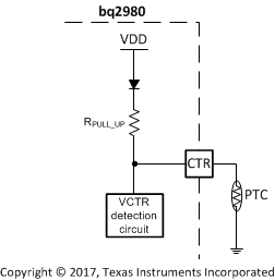
If any of the CTR pull-up resistors are selected, the device assumes a PTC is connected to the CTR pin. There are three internal pull-up options: 1.5 MΩ, 5 MΩ, or 8 MΩ. The internal pull-up allows a PTC to be connected between the CTR pin and VSS. This turns the CTR pin to detect an overtemperature fault through an external PTC, as shown in Figure 7-4.
 Figure 7-4 Connecting PTC to CTR Pin for Overtemperature Protection
When any of the CTR internal pull-up resistors are selected (factory configured), an active-high signal (VCTR > CTR VIH) on CTR turns off both CHG and DSG outputs, but it does not shut down the device.
As temperature goes up, the PTC resistance increases and when the voltage divided by the internal RPULL_UP and the RPTC is > CTR VIH, the CHG and DSG outputs are turned off. As temperature falls and the PTC resistance decreases, the CHG and DSG outputs turn back on when (VCTR < CTR VIL).