JAJSRJ8B September 2019 – October 2023 BQ75614-Q1
PRODUCTION DATA
- 1
- 1 特長
- 2 アプリケーション
- 3 概要
- 4 Revision History
- 5 概要 (続き)
- 6 Pin Configuration and Functions
- 7 Specifications
-
8 Detailed Description
- 8.1 Overview
- 8.2 Functional Block Diagram
- 8.3
Feature Description
- 8.3.1 Power Supplies
- 8.3.2 Measurement System
- 8.3.3 Cell Balancing
- 8.3.4 Integrated Hardware Protectors
- 8.3.5 GPIO Configuration
- 8.3.6
Communication, OTP, Diagnostic Control
- 8.3.6.1 Communication
- 8.3.6.2 Fault Handling
- 8.3.6.3 Nonvolatile Memory
- 8.3.6.4 Diagnostic Control/Status
- 8.4 Device Functional Modes
- 8.5
Register Maps
- 8.5.1 OTP Shadow Register Summary
- 8.5.2 Read/Write Register Summary
- 8.5.3 Read-Only Register Summary
- 8.5.4
Register Field Descriptions
- 8.5.4.1 Device Addressing Setup
- 8.5.4.2 Device ID and Scratch Pad
- 8.5.4.3 General Configuration and Control
- 8.5.4.4 Operation Status
- 8.5.4.5 ADC Configuration and Control
- 8.5.4.6
ADC Measurement Results
- 8.5.4.6.1 VCELL16_HI/LO
- 8.5.4.6.2 VCELL15_HI/LO
- 8.5.4.6.3 VCELL14_HI/LO
- 8.5.4.6.4 VCELL13_HI/LO
- 8.5.4.6.5 VCELL12_HI/LO
- 8.5.4.6.6 VCELL11_HI/LO
- 8.5.4.6.7 VCELL10_HI/LO
- 8.5.4.6.8 VCELL9_HI/LO
- 8.5.4.6.9 VCELL8_HI/LO
- 8.5.4.6.10 VCELL7_HI/LO
- 8.5.4.6.11 VCELL6_HI/LO
- 8.5.4.6.12 VCELL5_HI/LO
- 8.5.4.6.13 VCELL4_HI/LO
- 8.5.4.6.14 VCELL3_HI/LO
- 8.5.4.6.15 VCELL2_HI/LO
- 8.5.4.6.16 VCELL1_HI/LO
- 8.5.4.6.17 MAIN_CURRENT_HI/LO
- 8.5.4.6.18 CURRENT_HI/MID/LO
- 8.5.4.6.19 TSREF_HI/LO
- 8.5.4.6.20 GPIO1_HI/LO
- 8.5.4.6.21 GPIO2_HI/LO
- 8.5.4.6.22 GPIO3_HI/LO
- 8.5.4.6.23 GPIO4_HI/LO
- 8.5.4.6.24 GPIO5_HI/LO
- 8.5.4.6.25 GPIO6_HI/LO
- 8.5.4.6.26 GPIO7_HI/LO
- 8.5.4.6.27 GPIO8_HI/LO
- 8.5.4.6.28 DIETEMP1_HI/LO
- 8.5.4.6.29 DIETEMP2_HI/LO
- 8.5.4.6.30 AUX_CELL_HI/LO
- 8.5.4.6.31 AUX_GPIO_HI/LO
- 8.5.4.6.32 AUX_BAT_HI/LO
- 8.5.4.6.33 AUX_REFL_HI/LO
- 8.5.4.6.34 AUX_VBG2_HI/LO
- 8.5.4.6.35 AUX_AVAO_REF_HI/LO
- 8.5.4.6.36 AUX_AVDD_REF_HI/LO
- 8.5.4.6.37 AUX_OV_DAC_HI/LO
- 8.5.4.6.38 AUX_UV_DAC_HI/LO
- 8.5.4.6.39 AUX_OT_OTCB_DAC_HI/LO
- 8.5.4.6.40 AUX_UT_DAC_HI/LO
- 8.5.4.6.41 AUX_VCBDONE_DAC_HI/LO
- 8.5.4.6.42 AUX_VCM_HI/LO
- 8.5.4.6.43 REFOVDAC_HI/LO
- 8.5.4.6.44 DIAG_MAIN_HI/LO
- 8.5.4.6.45 DIAG_AUX_HI/LO
- 8.5.4.7 Balancing Configuration, Control and Status
- 8.5.4.8 Protector Configuration and Control
- 8.5.4.9 GPIO Configuration
- 8.5.4.10 SPI Master
- 8.5.4.11 Diagnostic Control
- 8.5.4.12 Fault Configuration and Reset
- 8.5.4.13
Fault Status
- 8.5.4.13.1 FAULT_SUMMARY
- 8.5.4.13.2 FAULT_COMM1
- 8.5.4.13.3 FAULT_OTP
- 8.5.4.13.4 FAULT_SYS
- 8.5.4.13.5 FAULT_PROT1
- 8.5.4.13.6 FAULT_PROT2
- 8.5.4.13.7 FAULT_OV1
- 8.5.4.13.8 FAULT_OV2
- 8.5.4.13.9 FAULT_UV1
- 8.5.4.13.10 FAULT_UV2
- 8.5.4.13.11 FAULT_OT
- 8.5.4.13.12 FAULT_UT
- 8.5.4.13.13 FAULT_COMP_GPIO
- 8.5.4.13.14 FAULT_COMP_VCCB1
- 8.5.4.13.15 FAULT_COMP_VCCB2
- 8.5.4.13.16 FAULT_COMP_VCOW1
- 8.5.4.13.17 FAULT_COMP_VCOW2
- 8.5.4.13.18 FAULT_COMP_CBOW1
- 8.5.4.13.19 FAULT_COMP_CBOW2
- 8.5.4.13.20 FAULT_COMP_CBFET1
- 8.5.4.13.21 FAULT_COMP_CBFET2
- 8.5.4.13.22 FAULT_COMP_MISC
- 8.5.4.13.23 FAULT_PWR1
- 8.5.4.13.24 FAULT_PWR2
- 8.5.4.13.25 FAULT_PWR3
- 8.5.4.14 Debug Control and Status
- 8.5.4.15
OTP Programming Control and Status
- 8.5.4.15.1 OTP_PROG_UNLOCK1A through OTP_PROG_UNLOCK1D
- 8.5.4.15.2 OTP_PROG_UNLOCK2A through OTP_PROG_UNLOCK2D
- 8.5.4.15.3 OTP_PROG_CTRL
- 8.5.4.15.4 OTP_ECC_TEST
- 8.5.4.15.5 OTP_ECC_DATAIN1 through OTP_ECC_DATAIN9
- 8.5.4.15.6 OTP_ECC_DATAOUT1 through OTP_ECC_DATAOUT9
- 8.5.4.15.7 OTP_PROG_STAT
- 8.5.4.15.8 OTP_CUST1_STAT
- 8.5.4.15.9 OTP_CUST2_STAT
- 9 Application and Implementation
- 10Power Supply Recommendations
- 11Layout
- 12Device and Documentation Support
- 13Mechanical, Packaging, and Orderable Information
9.2.1.2.2 Synchronize Voltage and Current Measurements
It is possible to synchronize the current and voltage measurements in the device. Both Voltage and current ADC start at the same time. CSADC conversion rate (Tconv) and ADC mode of operation (continuous or single run mode), time between reading voltage and current registers are some factors to consider when synchronizing the measurements.
Single run mode
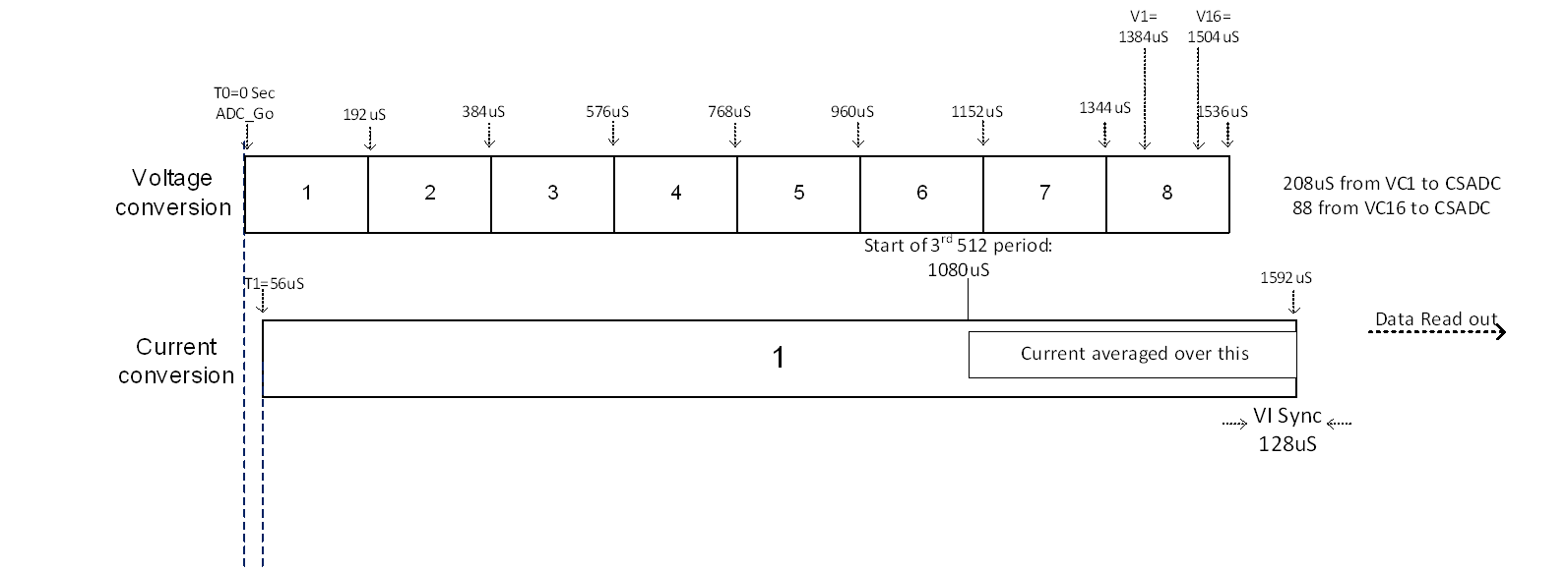
Figure 9-4 shows the case where single conversion happens at 3xTcs_conv where Tcs_conv = 512 μS and the CSADC stops. In this mode, the voltage ADC completes 8 round robin cycles and stops. The voltage and the current data conversions stop within 128 μS of each other. This can be considered the VI sync time in single conversion mode with above settings. The entire single run mode duration is much less than the settling of the voltage low pass filters. Hence the effect of filters can be ignored for this mode of operation.
 Figure 9-4 Single Conversion
Continuous run mode
When in continuous conversion mode, the voltage and the current ADCs are continuously running and constantly refreshing the contents of the results register after every conversion. The voltage and the current results registers have 89 registers between them. If the voltage and current are read out in a single read burst, the time that elapses between reading the voltage registers to reading the current register could be 1 mS. Hence for any Tcs_conv <=1 mS, the VI sync time between voltage and current conversion can be considered 1 mS.
Effect of Voltage Low Pass Filter in continuous run mode
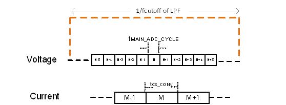
The Low pass filter in the voltage ADC path has fcutoff options of 6.5 Hz, 13 Hz, 26 Hz, 53 Hz, 111 Hz, 240 Hz, and 600 Hz, configurable through the ADC_CONF1[LPF_VCELL2:0] setting. The filters ensure that the voltage measurement is stable over a long period of time determined by the fcutoff. Since the voltage does not vary much within the filter time constant, it relaxes the requirement to read back the voltage and the current registers as close to each other as possible and gives MCU more time to read the results register. This is shown in Figure 9-5. Here the current conversion ‘M’ in the figure can be considered synced with voltage cycles around ‘M’ within ‘N-23’ and ‘N+23’ round robin cycles. The low pass filters are available in the voltage path, but not the current path which causes the two paths to have different frequency response. This needs to be accounted for in selection of filter fcutoff options and CSADC conversion rates.
