JAJSU42A April 2022 – April 2024 BQ76922
PRODUCTION DATA
- 1
- 1 特長
- 2 アプリケーション
- 3 概要
- 4 Device Comparison Table
- 5 Pin Configuration and Functions
-
6 Specifications
- 6.1 Absolute Maximum Ratings
- 6.2 ESD Ratings
- 6.3 Recommended Operating Conditions
- 6.4 Thermal Information BQ76922
- 6.5 Supply Current
- 6.6 Digital I/O
- 6.7 LD Pin
- 6.8 Precharge (PCHG) and Predischarge (PDSG) FET Drive
- 6.9 FUSE Pin Functionality
- 6.10 REG18 LDO
- 6.11 REG0 Pre-regulator
- 6.12 REG1 LDO
- 6.13 Voltage References
- 6.14 Coulomb Counter
- 6.15 Coulomb Counter Digital Filter (CC1)
- 6.16 Current Measurement Digital Filter (CC2)
- 6.17 Current Wake Detector
- 6.18 Analog-to-Digital Converter
- 6.19 Cell Balancing
- 6.20 Cell Open Wire Detector
- 6.21 Internal Temperature Sensor
- 6.22 Thermistor Measurement
- 6.23 Internal Oscillators
- 6.24 High-side NFET Drivers
- 6.25 Comparator-Based Protection Subsystem
- 6.26 Timing Requirements – I2C Interface, 100kHz Mode
- 6.27 Timing Requirements – I2C Interface, 400kHz Mode
- 6.28 Timing Requirements – HDQ Interface
- 6.29 Interface Timing Diagrams
- 6.30 Typical Characteristics
-
7 Detailed Description
- 7.1 Overview
- 7.2 Functional Block Diagram
- 7.3 Diagnostics
- 7.4 Device Configuration
- 7.5
Measurement Subsystem
- 7.5.1 Voltage Measurement
- 7.5.2 General Purpose ADCIN Functionality
- 7.5.3 Coulomb Counter and Digital Filters
- 7.5.4 Synchronized Voltage and Current Measurement
- 7.5.5 Internal Temperature Measurement
- 7.5.6 Thermistor Temperature Measurement
- 7.5.7 Factory Trim of Voltage ADC
- 7.5.8 Voltage Calibration (ADC Measurements)
- 7.5.9 Voltage Calibration (COV and CUV Protections)
- 7.5.10 Current Calibration
- 7.5.11 Temperature Calibration
- 7.6 Primary and Secondary Protection Subsystems
- 7.7
Device
Hardware Features
- 7.7.1 Voltage References
- 7.7.2 ADC Multiplexer
- 7.7.3 LDOs
- 7.7.4 Standalone Versus Host Interface
- 7.7.5 Multifunction Pin Controls
- 7.7.6 RST_SHUT Pin Operation
- 7.7.7 CFETOFF, DFETOFF, and BOTHOFF Pin Functionality
- 7.7.8 ALERT Pin Operation
- 7.7.9 Fuse Drive
- 7.7.10 Cell Open Wire
- 7.7.11 Low Frequency Oscillator
- 7.7.12 High Frequency Oscillator
- 7.8 Device Functional Modes
- 7.9 Serial Communications Interface
- 7.10 Cell Balancing
- 8 Application and Implementation
- 9 Power Supply Requirements
- 10Layout
- 11Device and Documentation Support
- 12Revision History
- 13Mechanical, Packaging, Orderable Information
パッケージ・オプション
デバイスごとのパッケージ図は、PDF版データシートをご参照ください。
メカニカル・データ(パッケージ|ピン)
- RSN|32
サーマルパッド・メカニカル・データ
発注情報
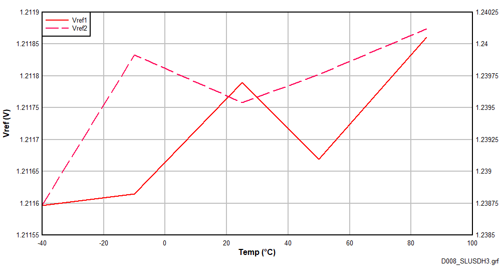
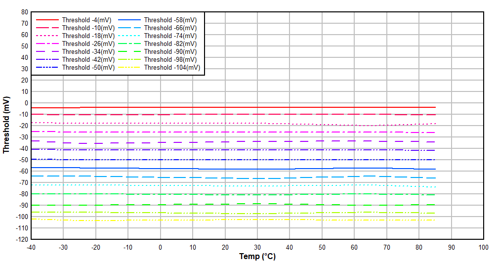
6.30 Typical Characteristics


Error in
measurement of differential voltage between SRP and SRN pins.
Figure 6-9 Current Measurement Error
vs
Temperature


 Figure 6-17 Cell Balancing Resistance
vs
Cell Common-mode Voltage at 25°C
 Figure 6-19 Thermistor Pullup
Resistance
vs
Temperature
(18-kΩ
Setting)
Error calculated as percentage of nominal gain
across
±200-mV
input range
Figure 6-21 Coulomb Counter Gain
Error
vs
Temperature Figure 6-23 REG18 Voltage
vs
Temperature
 Figure 6-25 BAT Current in NORMAL Mode
vs
Temperature
 Figure 6-27 BAT Current in SLEEP2 (SRC
Follower) Mode
vs
Temperature


LFO measured in
FULL
SPEED
mode (262 kHz)
Figure 6-12 Low Frequency Oscillator
(LFO) Accuracy
vs
Temperature
 Figure 6-16 Cell Balancing Resistance
vs
Temperature
 Figure 6-18 REG1 Voltage
vs
Load at 25°C
 Figure 6-20 Thermistor Pullup
Resistance
vs
Temperature
(180-kΩ
Setting)
 Figure 6-22 LD Wake Voltage
vs
Temperature
Measurements taken using external BJT
Figure 6-24 REGIN Voltage
vs
BAT Voltage Figure 6-26 BAT Current in SHUTDOWN Mode
vs
Temperature
 Figure 6-28 BAT Current in DEEPSLEEP2 (No
LFO) Mode
vs
Temperature