JAJSLR4E december 2012 – april 2021 BQ7716
PRODUCTION DATA
- 1
- 1 特長
- 2 アプリケーション
- 3 概要
- 4 Revision History
- 5 Device Comparison Table
- 6 Pin Configuration and Functions
- 7 Specifications
- 8 Detailed Description
- 9 Application and Implementation
- 10Power Supply Recommendations
- 11Layout
- 12Device and Documentation Support
- 13Mechanical, Packaging, and Orderable Information
6 Pin Configuration and Functions
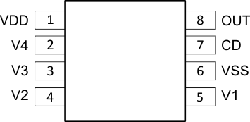
 Figure 6-1 DPJ Package8-Pin WSONTop View
Table 6-1 Pin Functions
| PIN | TYPE | DESCRIPTION | |
|---|---|---|---|
| NAME | NO. | I/O(1) | |
| CD | 7 | I/O | External capacitor connection for delay timer |
| OUT | 8 | OA | Output drive for overvoltage fault signal |
| VDD | 1 | P | Power supply |
| VSS | 6 | P | Electrically connected to IC ground and negative terminal of the lowest cell in the stack |
| V1 | 5 | I | Sense input for positive voltage of the lowest cell in the stack |
| V2 | 4 | I | Sense input for positive voltage of the second cell from the bottom of the stack |
| V3 | 3 | I | Sense input for positive voltage of the third cell from the bottom of the stack |
| V4 | 2 | I | Sense input for positive voltage of the fourth cell from the bottom of the stack |
(1) IA = Input Analog, OA = Output Analog, P = Power
Connection