JAJSQ30 june   2023 BQ79616

PRODUCTION DATA  

  1.   1
  2. 特長
  3. アプリケーション
  4. 概要
  5. Revision History
  6. 概要 (続き)
  7. Pin Configuration and Functions
  8. Specifications
    1. 7.1 Absolute Maximum Ratings
    2. 7.2 ESD Ratings
    3. 7.3 Recommended Operating Conditions
    4. 7.4 Thermal Information
    5. 7.5 Electrical Characteristics
    6. 7.6 Timing Requirements
    7. 7.7 Typical Characteristics
  9. Detailed Description
    1. 8.1 Overview
    2. 8.2 Functional Block Diagram
    3. 8.3 Feature Description
      1. 8.3.1 Power Supplies
        1. 8.3.1.1 AVAO_REF and AVDD_REF
        2. 8.3.1.2 LDOIN
        3. 8.3.1.3 AVDD
        4. 8.3.1.4 DVDD
        5. 8.3.1.5 CVDD and NEG5V
        6. 8.3.1.6 TSREF
      2. 8.3.2 Measurement System
        1. 8.3.2.1 Main ADC
          1. 8.3.2.1.1 Cell Voltage Measurements
            1. 8.3.2.1.1.1 Analog Front End
            2. 8.3.2.1.1.2 VC Channel Measurements
            3. 8.3.2.1.1.3 Post-ADC Digital LPF
            4. 8.3.2.1.1.4 BBP and BBN Measurements
          2. 8.3.2.1.2 Temperature Measurements
            1. 8.3.2.1.2.1 DieTemp1 Measurement
            2. 8.3.2.1.2.2 GPIOs and TSREF Measurements
          3. 8.3.2.1.3 Main ADC Operation Control
            1. 8.3.2.1.3.1 Operation Modes and Status
        2. 8.3.2.2 AUX ADC
          1. 8.3.2.2.1 AUX Cell Voltage Measurements
            1. 8.3.2.2.1.1 AUX Analog Front End
            2. 8.3.2.2.1.2 CB and BB Channel Measurements
          2. 8.3.2.2.2 AUX Temperature Measurements
            1. 8.3.2.2.2.1 DieTemp2 Measurement
            2. 8.3.2.2.2.2 AUX GPIO Measurements
          3. 8.3.2.2.3 MISC Measurements
          4. 8.3.2.2.4 AUX ADC Operation Control
        3. 8.3.2.3 Synchronization Between MAIN and AUX ADC Measurements
      3. 8.3.3 Cell Balancing
        1. 8.3.3.1 Set Up Cell Balancing
          1. 8.3.3.1.1 Step 1: Determine Balancing Channels
          2. 8.3.3.1.2 Step 2: Select Balancing Control Methods
          3. 8.3.3.1.3 Step 3a: Balancing Thermal Management
          4. 8.3.3.1.4 Step 3b: Option to Stop On Cell Voltage Threshold
          5. 8.3.3.1.5 Step 3c: Option to Stop at Fault
        2. 8.3.3.2 Cell Balancing in SLEEP Mode
        3. 8.3.3.3 Pause and Stop Cell Balancing
          1. 8.3.3.3.1 Cell Balancing Pause
          2. 8.3.3.3.2 Cell Balancing Stop
          3. 8.3.3.3.3 Remaining CB Time
        4. 8.3.3.4 Module Balancing
          1. 8.3.3.4.1 Start Module Balancing
          2. 8.3.3.4.2 Stop Module Balancing
      4. 8.3.4 Integrated Hardware Protectors
        1. 8.3.4.1 OVUV Protectors
          1. 8.3.4.1.1 OVUV Operation Modes
          2. 8.3.4.1.2 OVUV Control and Status
            1. 8.3.4.1.2.1 OVUV Control
            2. 8.3.4.1.2.2 OVUV Status
        2. 8.3.4.2 OTUT Protector
          1. 8.3.4.2.1 OTUT Operation Modes
          2. 8.3.4.2.2 OTUT Control and Status
            1. 8.3.4.2.2.1 OTUT Control
            2. 8.3.4.2.2.2 OTUT Status
      5. 8.3.5 GPIO Configuration
      6. 8.3.6 Communication, OTP, Diagnostic Control
        1. 8.3.6.1 Communication
          1. 8.3.6.1.1 Serial Interface
            1. 8.3.6.1.1.1 UART Physical Layer
              1. 8.3.6.1.1.1.1 UART Transmitter
              2. 8.3.6.1.1.1.2 UART Receiver
              3. 8.3.6.1.1.1.3 COMM CLEAR
            2. 8.3.6.1.1.2 Command and Response Protocol
              1. 8.3.6.1.1.2.1 Transaction Frame Structure
                1. 8.3.6.1.1.2.1.1 Frame Initialization Byte
                2. 8.3.6.1.1.2.1.2 Device Address Byte
                3. 8.3.6.1.1.2.1.3 Register Address Bytes
                4. 8.3.6.1.1.2.1.4 Data Bytes
                5. 8.3.6.1.1.2.1.5 CRC Bytes
                6. 8.3.6.1.1.2.1.6 Calculating Frame CRC Value
                7. 8.3.6.1.1.2.1.7 Verifying Frame CRC
              2. 8.3.6.1.1.2.2 Transaction Frame Examples
                1. 8.3.6.1.1.2.2.1 Single Device Read/Write
                2. 8.3.6.1.1.2.2.2 Stack Read/Write
                3. 8.3.6.1.1.2.2.3 Broadcast Read/Write
                4. 8.3.6.1.1.2.2.4 Broadcast Write Reverse Direction
          2. 8.3.6.1.2 Daisy Chain Interface
            1. 8.3.6.1.2.1 Daisy Chain Transmitter and Receiver Functionality
            2. 8.3.6.1.2.2 Daisy Chain Protocol
          3. 8.3.6.1.3 Start Communication
            1. 8.3.6.1.3.1 Identify Base and Stack
            2. 8.3.6.1.3.2 Auto-Addressing
              1. 8.3.6.1.3.2.1 Setting Up the Device Addresses
              2. 8.3.6.1.3.2.2 Setting Up COMM_CTRL[STACK_DEV] and [TOP_STACK]
              3. 8.3.6.1.3.2.3 Storing Device Address to OTP
            3. 8.3.6.1.3.3 Synchronize Daisy Chain DLL
            4. 8.3.6.1.3.4 Ring Communication
          4. 8.3.6.1.4 Communication Timeout
            1. 8.3.6.1.4.1 Short Communication Timeout
            2. 8.3.6.1.4.2 Long Communication Timeout
          5. 8.3.6.1.5 Communication Debug Mode
          6. 8.3.6.1.6 Multidrop Configuration
          7. 8.3.6.1.7 SPI Controller
          8. 8.3.6.1.8 SPI Loopback
        2. 8.3.6.2 Fault Handling
          1. 8.3.6.2.1 Fault Status Hierarchy
            1. 8.3.6.2.1.1 Debug Registers
          2. 8.3.6.2.2 Fault Masking and Reset
            1. 8.3.6.2.2.1 Fault Masking
            2. 8.3.6.2.2.2 Fault Reset
          3. 8.3.6.2.3 Fault Signaling
            1. 8.3.6.2.3.1 Fault Status Transmitting in ACTIVE Mode
            2. 8.3.6.2.3.2 Fault Status Transmitting in SLEEP Mode
            3. 8.3.6.2.3.3 Heartbeat and Fault Tone
        3. 8.3.6.3 Nonvolatile Memory
          1. 8.3.6.3.1 OTP Page Status
          2. 8.3.6.3.2 OTP Programming
        4. 8.3.6.4 Diagnostic Control/Status
          1. 8.3.6.4.1 Power Supplies Check
            1. 8.3.6.4.1.1 Power Supply Diagnostic Check
            2. 8.3.6.4.1.2 Power Supply BIST
          2. 8.3.6.4.2 Thermal Shutdown and Warning Check
            1. 8.3.6.4.2.1 Thermal Shutdown
            2. 8.3.6.4.2.2 Thermal Warning
          3. 8.3.6.4.3 Oscillators Watchdog
          4. 8.3.6.4.4 OTP Error Check
            1. 8.3.6.4.4.1 OTP CRC Test and Faults
            2. 8.3.6.4.4.2 OTP Margin Read
            3. 8.3.6.4.4.3 Error Check and Correct (ECC) OTP
          5. 8.3.6.4.5 Integrated Hardware Protector Check
            1. 8.3.6.4.5.1 Parity Check
            2. 8.3.6.4.5.2 OVUV and OTUT DAC Check
            3. 8.3.6.4.5.3 OVUV Protector BIST
            4. 8.3.6.4.5.4 OTUT Protector BIST
          6. 8.3.6.4.6 Diagnostic Through ADC Comparison
            1. 8.3.6.4.6.1 Cell Voltage Measurement Check
            2. 8.3.6.4.6.2 Temperature Measurement Check
            3. 8.3.6.4.6.3 Cell Balancing FETs Check
            4. 8.3.6.4.6.4 VC and CB Open Wire Check
      7. 8.3.7 Bus Bar Support
        1. 8.3.7.1 Bus Bar on BBP/BBN Pins
          1. 8.3.7.1.1 Typical Connection
          2. 8.3.7.1.2 Bus Bar Measurement
          3. 8.3.7.1.3 Cell Balancing Handling
          4. 8.3.7.1.4 Cell Voltage Diagnostic Control
        2. 8.3.7.2 Bus Bar on Individual VC Channel
          1. 8.3.7.2.1 Typical Connection
          2. 8.3.7.2.2 Bus Bar Measurement
          3. 8.3.7.2.3 Cell Balancing Handling
          4. 8.3.7.2.4 Cell Voltage Diagnostic Control
    4. 8.4 Device Functional Modes
      1. 8.4.1 Power Modes
        1. 8.4.1.1 SHUTDOWN Mode
          1. 8.4.1.1.1 Exit SHUTDOWN Mode
          2. 8.4.1.1.2 Enter SHUTDOWN Mode
        2. 8.4.1.2 SLEEP Mode
          1. 8.4.1.2.1 Exit SLEEP Mode
          2. 8.4.1.2.2 Enter SLEEP Mode
        3. 8.4.1.3 ACTIVE Mode
          1. 8.4.1.3.1 Exit ACTIVE Mode
          2. 8.4.1.3.2 Enter ACTIVE Mode from SHUTDOWN Mode
          3. 8.4.1.3.3 Enter ACTIVE Mode from SLEEP Mode
      2. 8.4.2 Device Reset
      3. 8.4.3 Ping and Tone
        1. 8.4.3.1 Ping
        2. 8.4.3.2 Tone
        3. 8.4.3.3 Ping and Tone Propagation
    5. 8.5 Register Maps
      1. 8.5.1 OTP Shadow Register Summary
      2. 8.5.2 Read/Write Register Summary
      3. 8.5.3 Read-Only Register Summary
      4. 8.5.4 Register Field Descriptions
        1. 8.5.4.1  Device Addressing Setup
          1. 8.5.4.1.1 DIR0_ADDR_OTP
          2. 8.5.4.1.2 DIR1_ADDR_OTP
          3. 8.5.4.1.3 CUST_MISC1 through CUST_MISC8
          4. 8.5.4.1.4 DIR0_ADDR
          5. 8.5.4.1.5 DIR1_ADDR
        2. 8.5.4.2  Device ID and Scratch Pad
          1. 8.5.4.2.1 PARTID
          2. 8.5.4.2.2 DEV_REVID
          3. 8.5.4.2.3 DIE_ID1 through DIE_ID9
        3. 8.5.4.3  General Configuration and Control
          1. 8.5.4.3.1  DEV_CONF
          2. 8.5.4.3.2  ACTIVE_CELL
          3. 8.5.4.3.3  BBVC_POSN1
          4. 8.5.4.3.4  BBVC_POSN2
          5. 8.5.4.3.5  PWR_TRANSIT_CONF
          6. 8.5.4.3.6  COMM_TIMEOUT_CONF
          7. 8.5.4.3.7  TX_HOLD_OFF
          8. 8.5.4.3.8  STACK_RESPONSE
          9. 8.5.4.3.9  BBP_LOC
          10. 8.5.4.3.10 COMM_CTRL
          11. 8.5.4.3.11 CONTROL1
          12. 8.5.4.3.12 CONTROL2
          13. 8.5.4.3.13 CUST_CRC_HI
          14. 8.5.4.3.14 CUST_CRC_LO
          15. 8.5.4.3.15 CUST_CRC_RSLT_HI
          16. 8.5.4.3.16 CUST_CRC_RSLT_LO
        4. 8.5.4.4  Operation Status
          1. 8.5.4.4.1 DIAG_STAT
          2. 8.5.4.4.2 ADC_STAT1
          3. 8.5.4.4.3 ADC_STAT2
          4. 8.5.4.4.4 GPIO_STAT
          5. 8.5.4.4.5 BAL_STAT
          6. 8.5.4.4.6 DEV_STAT
        5. 8.5.4.5  ADC Configuration and Control
          1. 8.5.4.5.1 ADC_CONF1
          2. 8.5.4.5.2 ADC_CONF2
          3. 8.5.4.5.3 MAIN_ADC_CAL1
          4. 8.5.4.5.4 MAIN_ADC_CAL2
          5. 8.5.4.5.5 AUX_ADC_CAL1
          6. 8.5.4.5.6 AUX_ADC_CAL2
          7. 8.5.4.5.7 ADC_CTRL1
          8. 8.5.4.5.8 ADC_CTRL2
          9. 8.5.4.5.9 ADC_CTRL3
        6. 8.5.4.6  ADC Measurement Results
          1. 8.5.4.6.1  VCELL16_HI/LO
          2. 8.5.4.6.2  VCELL15_HI/LO
          3. 8.5.4.6.3  VCELL14_HI/LO
          4. 8.5.4.6.4  VCELL13_HI/LO
          5. 8.5.4.6.5  VCELL12_HI/LO
          6. 8.5.4.6.6  VCELL11_HI/LO
          7. 8.5.4.6.7  VCELL10_HI/LO
          8. 8.5.4.6.8  VCELL9_HI/LO
          9. 8.5.4.6.9  VCELL8_HI/LO
          10. 8.5.4.6.10 VCELL7_HI/LO
          11. 8.5.4.6.11 VCELL6_HI/LO
          12. 8.5.4.6.12 VCELL5_HI/LO
          13. 8.5.4.6.13 VCELL4_HI/LO
          14. 8.5.4.6.14 VCELL3_HI/LO
          15. 8.5.4.6.15 VCELL2_HI/LO
          16. 8.5.4.6.16 VCELL1_HI/LO
          17. 8.5.4.6.17 BUSBAR_HI/LO
          18. 8.5.4.6.18 TSREF_HI/LO
          19. 8.5.4.6.19 GPIO1_HI/LO
          20. 8.5.4.6.20 GPIO2_HI/LO
          21. 8.5.4.6.21 GPIO3_HI/LO
          22. 8.5.4.6.22 GPIO4_HI/LO
          23. 8.5.4.6.23 GPIO5_HI/LO
          24. 8.5.4.6.24 GPIO6_HI/LO
          25. 8.5.4.6.25 GPIO7_HI/LO
          26. 8.5.4.6.26 GPIO8_HI/LO
          27. 8.5.4.6.27 DIETEMP1_HI/LO
          28. 8.5.4.6.28 DIETEMP2_HI/LO
          29. 8.5.4.6.29 AUX_CELL_HI/LO
          30. 8.5.4.6.30 AUX_GPIO_HI/LO
          31. 8.5.4.6.31 AUX_BAT_HI/LO
          32. 8.5.4.6.32 AUX_REFL_HI/LO
          33. 8.5.4.6.33 AUX_VBG2_HI/LO
          34. 8.5.4.6.34 AUX_AVAO_REF_HI/LO
          35. 8.5.4.6.35 AUX_AVDD_REF_HI/LO
          36. 8.5.4.6.36 AUX_OV_DAC_HI/LO
          37. 8.5.4.6.37 AUX_UV_DAC_HI/LO
          38. 8.5.4.6.38 AUX_OT_OTCB_DAC_HI/LO
          39. 8.5.4.6.39 AUX_UT_DAC_HI/LO
          40. 8.5.4.6.40 AUX_VCBDONE_DAC_HI/LO
          41. 8.5.4.6.41 AUX_VCM_HI/LO
          42. 8.5.4.6.42 REFOVDAC_HI/LO
          43. 8.5.4.6.43 DIAG_MAIN_HI/LO
          44. 8.5.4.6.44 DIAG_AUX_HI/LO
        7. 8.5.4.7  Balancing Configuration, Control and Status
          1. 8.5.4.7.1  CB_CELL16_CTRL through CB_CELL1_CTRL
          2. 8.5.4.7.2  VMB_DONE_THRESH
          3. 8.5.4.7.3  MB_TIMER_CTRL
          4. 8.5.4.7.4  VCB_DONE_THRESH
          5. 8.5.4.7.5  OTCB_THRESH
          6. 8.5.4.7.6  BAL_CTRL1
          7. 8.5.4.7.7  BAL_CTRL2
          8. 8.5.4.7.8  BAL_CTRL3
          9. 8.5.4.7.9  CB_COMPLETE1
          10. 8.5.4.7.10 CB_COMPLETE2
          11. 8.5.4.7.11 BAL_TIME
        8. 8.5.4.8  Protector Configuration and Control
          1. 8.5.4.8.1 OV_THRESH
          2. 8.5.4.8.2 UV_THRESH
          3. 8.5.4.8.3 UV_DISABLE1
          4. 8.5.4.8.4 UV_DISABLE2
          5. 8.5.4.8.5 OTUT_THRESH
          6. 8.5.4.8.6 OVUV_CTRL
          7. 8.5.4.8.7 OTUT_CTRL
        9. 8.5.4.9  GPIO Configuration
          1. 8.5.4.9.1 GPIO_CONF1
          2. 8.5.4.9.2 GPIO_CONF2
          3. 8.5.4.9.3 GPIO_CONF3
          4. 8.5.4.9.4 GPIO_CONF4
        10. 8.5.4.10 SPI Controller
          1. 8.5.4.10.1 SPI_CONF
          2. 8.5.4.10.2 SPI_EXE
          3. 8.5.4.10.3 SPI_TX3, SPI_TX2, and SPI_TX1
          4. 8.5.4.10.4 SPI_RX3, SPI_RX2, and SPI_RX1
        11. 8.5.4.11 Diagnostic Control
          1. 8.5.4.11.1  DIAG_OTP_CTRL
          2. 8.5.4.11.2  DIAG_COMM_CTRL
          3. 8.5.4.11.3  DIAG_PWR_CTRL
          4. 8.5.4.11.4  DIAG_CBFET_CTRL1
          5. 8.5.4.11.5  DIAG_CBFET_CTRL2
          6. 8.5.4.11.6  DIAG_COMP_CTRL1
          7. 8.5.4.11.7  DIAG_COMP_CTRL2
          8. 8.5.4.11.8  DIAG_COMP_CTRL3
          9. 8.5.4.11.9  DIAG_COMP_CTRL4
          10. 8.5.4.11.10 DIAG_PROT_CTRL
        12. 8.5.4.12 Fault Configuration and Reset
          1. 8.5.4.12.1 FAULT_MSK1
          2. 8.5.4.12.2 FAULT_MSK2
          3. 8.5.4.12.3 FAULT_RST1
          4. 8.5.4.12.4 FAULT_RST2
        13. 8.5.4.13 Fault Status
          1. 8.5.4.13.1  FAULT_SUMMARY
          2. 8.5.4.13.2  FAULT_COMM1
          3. 8.5.4.13.3  FAULT_COMM2
          4. 8.5.4.13.4  FAULT_COMM3
          5. 8.5.4.13.5  FAULT_OTP
          6. 8.5.4.13.6  FAULT_SYS
          7. 8.5.4.13.7  FAULT_PROT1
          8. 8.5.4.13.8  FAULT_PROT2
          9. 8.5.4.13.9  FAULT_OV1
          10. 8.5.4.13.10 FAULT_OV2
          11. 8.5.4.13.11 FAULT_UV1
          12. 8.5.4.13.12 FAULT_UV2
          13. 8.5.4.13.13 FAULT_OT
          14. 8.5.4.13.14 FAULT_UT
          15. 8.5.4.13.15 FAULT_COMP_GPIO
          16. 8.5.4.13.16 FAULT_COMP_VCCB1
          17. 8.5.4.13.17 FAULT_COMP_VCCB2
          18. 8.5.4.13.18 FAULT_COMP_VCOW1
          19. 8.5.4.13.19 FAULT_COMP_VCOW2
          20. 8.5.4.13.20 FAULT_COMP_CBOW1
          21. 8.5.4.13.21 FAULT_COMP_CBOW2
          22. 8.5.4.13.22 FAULT_COMP_CBFET1
          23. 8.5.4.13.23 FAULT_COMP_CBFET2
          24. 8.5.4.13.24 FAULT_COMP_MISC
          25. 8.5.4.13.25 FAULT_PWR1
          26. 8.5.4.13.26 FAULT_PWR2
          27. 8.5.4.13.27 FAULT_PWR3
        14. 8.5.4.14 Debug Control and Status
          1. 8.5.4.14.1  DEBUG_CTRL_UNLOCK
          2. 8.5.4.14.2  DEBUG_COMM_CTRL1
          3. 8.5.4.14.3  DEBUG_COMM_CTRL2
          4. 8.5.4.14.4  DEBUG_COMM_STAT
          5. 8.5.4.14.5  DEBUG_UART_RC
          6. 8.5.4.14.6  DEBUG_UART_RR_TR
          7. 8.5.4.14.7  DEBUG_COMH_BIT
          8. 8.5.4.14.8  DEBUG_COMH_RC
          9. 8.5.4.14.9  DEBUG_COMH_RR_TR
          10. 8.5.4.14.10 DEBUG_COML_BIT
          11. 8.5.4.14.11 DEBUG_COML_RC
          12. 8.5.4.14.12 DEBUG_COML_RR_TR
          13. 8.5.4.14.13 DEBUG_UART_DISCARD
          14. 8.5.4.14.14 DEBUG_COMH_DISCARD
          15. 8.5.4.14.15 DEBUG_COML_DISCARD
          16. 8.5.4.14.16 DEBUG_UART_VALID_HI/LO
          17. 8.5.4.14.17 DEBUG_COMH_VALID_HI/LO
          18. 8.5.4.14.18 DEBUG_COML_VALID_HI/LO
          19. 8.5.4.14.19 DEBUG_OTP_SEC_BLK
          20. 8.5.4.14.20 DEBUG_OTP_DED_BLK
        15. 8.5.4.15 OTP Programming Control and Status
          1. 8.5.4.15.1 OTP_PROG_UNLOCK1A through OTP_PROG_UNLOCK1D
          2. 8.5.4.15.2 OTP_PROG_UNLOCK2A through OTP_PROG_UNLOCK2D
          3. 8.5.4.15.3 OTP_PROG_CTRL
          4. 8.5.4.15.4 OTP_ECC_TEST
          5. 8.5.4.15.5 OTP_ECC_DATAIN1 through OTP_ECC_DATAIN9
          6. 8.5.4.15.6 OTP_ECC_DATAOUT1 through OTP_ECC_DATAOUT9
          7. 8.5.4.15.7 OTP_PROG_STAT
          8. 8.5.4.15.8 OTP_CUST1_STAT
          9. 8.5.4.15.9 OTP_CUST2_STAT
  10. Application and Implementation
    1. 9.1 Application Information
    2. 9.2 Typical Applications
      1. 9.2.1 Base Device Application Circuit
        1. 9.2.1.1 Design Requirements
        2. 9.2.1.2 Detailed Design Procedure
          1. 9.2.1.2.1 Cell Sensing and Balancing Inputs
          2. 9.2.1.2.2 BAT and External NPN
          3. 9.2.1.2.3 Power Supplies, Reference Input
          4. 9.2.1.2.4 GPIO For Thermistor Inputs
          5. 9.2.1.2.5 Internal Balancing Current
          6. 9.2.1.2.6 UART, NFAULT
          7. 9.2.1.2.7 Daisy Chain Isolation
            1. 9.2.1.2.7.1 Devices Connected on the Same PCB
            2. 9.2.1.2.7.2 Devices Connected on Different PCBs
        3. 9.2.1.3 Application Curve
      2. 9.2.2 Daisy Device Application Circuit
        1. 9.2.2.1 Design Requirements
        2. 9.2.2.2 Detailed Design Procedure
  11. 10Power Supply Recommendations
  12. 11Layout
    1. 11.1 Layout Guidelines
      1. 11.1.1 Ground Planes
      2. 11.1.2 Bypass Capacitors for Power Supplies and Reference
      3. 11.1.3 Cell Voltage Sensing
      4. 11.1.4 Daisy Chain Communication
    2. 11.2 Layout Example
  13. 12Device and Documentation Support
    1. 12.1 Device Support
      1. 12.1.1 サード・パーティ製品に関する免責事項
    2. 12.2 ドキュメントの更新通知を受け取る方法
    3. 12.3 サポート・リソース
    4. 12.4 Trademarks
    5. 12.5 静電気放電に関する注意事項
    6. 12.6 用語集
  14. 13Mechanical, Packaging, and Orderable Information

パッケージ・オプション

メカニカル・データ(パッケージ|ピン)
サーマルパッド・メカニカル・データ
発注情報
BAT and External NPN
Related PinsComponentsValueDescription
BATFilter resistor30 ΩSingle-ended RC filter, recommended values must be used for hot-plug performance.
Filter capacitor10 nF/100 V
Can use lower voltage rating based on module size
NPNBNPN (Q1)Collector–emitter breakdown voltage 80 V to 100 V, but can use lower rating based on module size
Power rating ≥ 1 W
Gain > 80 at the expected load current
Current handling >100 mA
The external NPN is used to form a preregulation circuit to provide a 6-V (typical) input to the LDOIN pin.
The voltage rating of the NPN can be optimized by the following equation:
NPN voltage rating = Max VModule – Min VLDOIN + Margin
Where:
Max VModule = maximum module voltage with fully charged cells
Min VLDOIN = the minimum spec of the VLDOIN parameter
Margin = system transient voltage + design margin per application requirement
Resistor on external NPN collector (RNPN)Various based on module voltageThe resistor has a couple purposes:
(a) For an RC filter for the NPN preregulation circuit
(b) Share the thermal dissipation with the NPN
Capacitor on external NPN collector0.22 μF/100 V
Can use lower voltage rating based on module size
The capacitor forms the RC filter for the NPN preregulation circuit
The capacitor rating is based on peak voltage spike seen on the module. For smaller module size, < 100-V rated capacitor can be used. System designer selects the optimized voltage-rated capacitor per their system tolerance and requirements.

To reduce the power rating needed for the external NPN (Q1), system designers can put power resistors on the NPN collector to create an IR drop from the module voltage (VModule). Figure 9-3 shows the current paths to power the BQ79616 device.

Typical ISTARTUP current, that is, inrush startup current when the device enters from SHUTDOWN to ACTIVE, is 20 mA for TI recommended components. This current is the sum of IBAT + ILDOIN, and is dependent on PCB board components and layout. Designers must characterize this on their end.
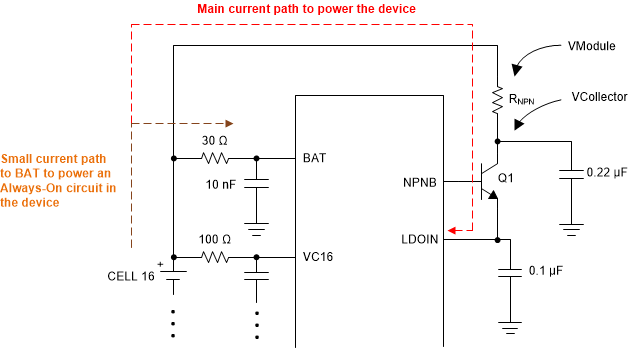
GUID-005BCD4E-500F-4A6D-850E-52E35B4D3AF2-low.gifFigure 9-3 Power Consumption Paths

To ensure there is sufficient headroom to maintain 6 V (typical) regulated voltage on LDOIN pin, system designer ensures VCollector has ≥ 8 V at any time with the assumption of about 2-V drop across the NPN.

Therefore, maximum allowable RNPN value = ((Min VModule) – (VCollector)) / (Max peak current)

Where:

Min VModule: based on module size and minimum cell voltage per application

VCollector: 8 V with the assumption of about 2-V drop across NPN

Max peak current: highest operation current, which is the active current with all functions turned on. Note that different communication isolation components (for example, capacitor isolation versus transformer, or the type of transformer) contribute different loading to the total power consumption.

Powering the device separately from the top of the battery stack:

The device is designed to be powered by the battery stack. If there is a need to power the device from a separate source such as in Figure 9-4, the following relationship between the voltage on the BAT pin and the highest VC pin voltage (with respected to ground) is BAT voltage ≥ (0.5 × highest VC voltage) + 2.

For example, if the device is connected to a 14S module with max cell voltage of 4.2 V/cell, the highest VC pin is VC14, and the highest VC14 voltage is (4.2 V × 14) = 58.8 V. If the BAT pin is powered separately, BAT voltage must be ≥ 31.4 V.

Similarly, if BBP/N channel is connected above the highest cell stack, the BBP pin will has the highest voltage (with respected to ground) than the VC pins. In this scenario, VBAT ≥ [(VBBP-2.5) × 0.84] + 4.5. The requirement applies when BAT is power separately and it is to ensure proper operation of the internal level shifter. Fail to maintain the voltage relationship will increase the ADC measurement error on the VC and BB channels.
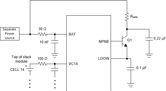
GUID-D39C19BA-CFA1-4556-B3A0-99F94C647662-low.gifFigure 9-4 Separate Power Source to BAT