JAJSEK1C August 2011 – August 2018 BUF20800-Q1
PRODUCTION DATA.
- 1 特長
- 2 アプリケーション
- 3 概要
- 4 改訂履歴
- 5 Pin Configuration and Functions
- 6 Specifications
- 7 Detailed Description
- 8 Application and Implementation
- 9 Power Supply Recommendations
- 10Layout
- 11デバイスおよびドキュメントのサポート
- 12メカニカル、パッケージ、および注文情報
パッケージ・オプション
メカニカル・データ(パッケージ|ピン)
- DCP|38
サーマルパッド・メカニカル・データ
- DCP|38
発注情報
7.5.3.2 Reading
Reading a DAC register will return the data stored in the DAC. This data can differ from the data stored in the DAC register. See the Output Latch section.
To read the DAC value:
- Send a START condition on the bus.
- Send the device address and read/write bit = LOW. The BUF20800-Q1 will acknowledge this byte.
- Send the DAC address byte. Bits D7−D5 must be set to 0; Bits D4−D0 are the DAC address. Only DAC addresses 00000 to 10011 are valid and will be acknowledged.
- Send a START or STOP/START condition on the bus.
- Send correct device address and read/write bit = HIGH. The BUF20800-Q1 will acknowledge this byte.
- Receive two bytes of data. They are for the specified DAC. The first received byte is the most significant byte (bits D15−D8; only bits D9 and D8 have meaning); the next byte is the least significant byte (bits D7−D0).
- Acknowledge after receiving the first byte.
- Do not acknowledge the second byte to end the read transaction.
Communication may be terminated by sending a premature STOP or START condition on the bus, or by not sending the acknowledge.
To Read Multiple DACs:
- Send a START condition on the bus.
- Send the device address and read/write bit = LOW. The BUF20800-Q1 will acknowledge this byte.
- Send either the DAC_1 address byte to start at the first DAC, or send the address byte for whichever DAC will be the first in the sequence of DACs to be read. The BUF20800-Q1 will begin with this DAC and step through subsequent DACs in sequential order.
- Send a START or STOP/START condition on the bus.
- Send correct device address and read/write bit = HIGH. The BUF20800-Q1 will acknowledge this byte.
- Receive two bytes of data. They are for the specified DAC. The first received byte is the most significant byte (bits D15−D8, only bits D9 and D8 have meaning); the next byte is the least significant byte (bits D7−D0).
- Acknowledge after receiving each byte of data except for the last byte. The acknowledge bit of the last byte should be HIGH to end the read operation.
- When all desired DACs have been read, send a STOP or repeated START condition on the bus.
Communication may be terminated by sending a premature STOP or START condition on the bus, or by not sending the acknowledge.
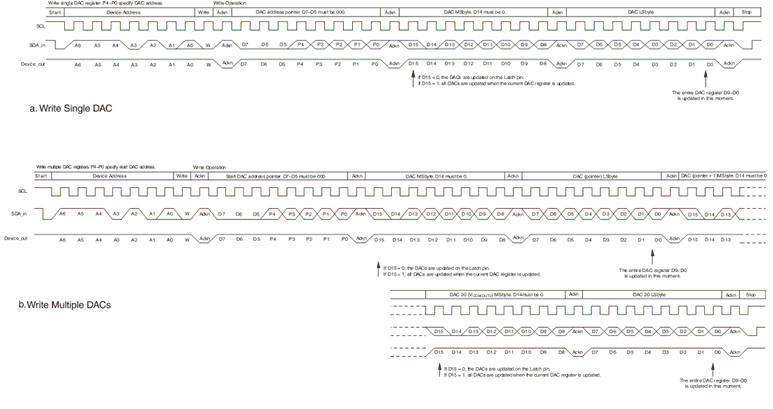
 Figure 12. Timing Diagram for Write DAC Register
  Figure 13. Timing Diagram for Read DAC Register