JAJSMA5C June 2021 – March 2022 BUF802
PRODUCTION DATA
- 1 特長
- 2 アプリケーション
- 3 説明
- 4 Revision History
- 5 Pin Configuration and Functions
- 6 Specifications
- 7 Parameter Measurement Information
- 8 Detailed Description
- 9 Application and Implementation
- 10Power Supply Recommendations
- 11Layout
- 12Device and Documentation Support
- 13Mechanical, Packaging, and Orderable Information
パッケージ・オプション
メカニカル・データ(パッケージ|ピン)
- RGT|16
サーマルパッド・メカニカル・データ
- RGT|16
発注情報
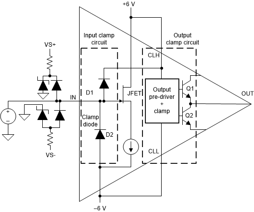
8.3.1 Input and Output Over-Voltage Clamp
 Figure 8-2 Internal Input and Output
Over-Voltage Clamp
Figure 8-2 Internal Input and Output
Over-Voltage ClampThe BUF802 device integrates an input and output clamp circuit. The input clamp protects the BUF802 from large input transients and the output clamp protects the subsequent stages from being overdriven.
- Input Clamp Circuit:
- Figure 8-2 shows the input of the BUF802 tied to pins CLH and VS- through two internal clamp diodes, D1 and D2. The diodes are rated for 100 mA of continuous current but can withstand much higher transient currents. If the JFET input voltage exceeds the voltage at CLH or VS-, the diodes get forward biased, clamping the JFET to CLH and VS-. A 1 μF capacitor connected in parallel to the zener diode, helps in transient absorption travelling through the D1 diode.
- Figure 8-3 shows how the external clamping diodes can be used in cases where the 100 mA current rating of D1 and D2 is insufficient. When using external clamping, disable the internal protection of the BUF802 by connecting CLH and CLL to VS+ and VS-.
 Figure 8-3 External Input Clamp Circuit
- Output Clamp Circuit:
- The output protection circuit prevents the stages following the BUF802 from being overdriven and also ensures that the BUF802 recovers rapidly from a saturated state resulting from an input or output overdrive condition. In a typical data-acquisition system, the BUF802 would be followed by a variable gain amplifier (VGA). High-speed VGAs are typically designed on 5 V processes making it susceptible to potential damage from the 12 V BUF802. The voltage applied to the CLH and CLL pins dictate the maximum output swing of the BUF802.
- As shown in Figure 8-3, the internal clamps can be disabled by connecting CLH and CLL to VS+ and VS- respectively. When the clamps are disabled, the maximum output swing is limited by the output swing specification described in Section 6.5. The response time and accuracy of the output clamp is shown in Section 6.7.
- The output THD of the BUF802 degrades when VCLH and VCLL are set close to the expected VOUT peak value. To prevent signal degradation, maintain at least a 1.5 V difference between the expected peak output voltage and the clamp voltage applied at the CLH and CLL pins. Figure 8-4 shows the relation between the absolute clamp voltage value and THD for a 1 VPP output.
Figure 8-4 THD vs VCLH /
VCLL for VOUT = 1 VPP
Figure 8-5 Transient Clamp
Response