JAJSHI1B February 2019 – May 2021 CC3135
PRODUCTION DATA
- 1 特長
- 2 アプリケーション
- 3 概要
- 4 機能ブロック図
- 5 Revision History
- 6 Device Comparison
- 7 Terminal Configuration and Functions
-
8 Specifications
- 8.1 Absolute Maximum Ratings
- 8.2 ESD Ratings
- 8.3 Power-On Hours (POH)
- 8.4 Recommended Operating Conditions
- 8.5 Current Consumption Summary: 2.4 GHz RF Band
- 8.6 Current Consumption Summary: 5 GHz RF Band
- 8.7 TX Power Control for 2.4 GHz Band
- 8.8 TX Power Control for 5 GHz
- 8.9 Brownout and Blackout Conditions
- 8.10 Electrical Characteristics for DIO Pins
- 8.11 Electrical Characteristics for Pin Internal Pullup and Pulldown
- 8.12 WLAN Receiver Characteristics
- 8.13 WLAN Transmitter Characteristics
- 8.14 WLAN Transmitter Out-of-Band Emissions
- 8.15 BLE/2.4 GHz Radio Coexistence and WLAN Coexistence Requirements
- 8.16 Thermal Resistance Characteristics for RGK Package
- 8.17 Timing and Switching Characteristics
- 8.18 External Interfaces
- 9 Detailed Description
- 10Applications, Implementation, and Layout
- 11Device and Documentation Support
- 12Mechanical, Packaging, and Orderable Information
10.1.3 Typical Application
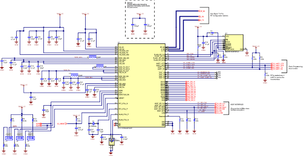
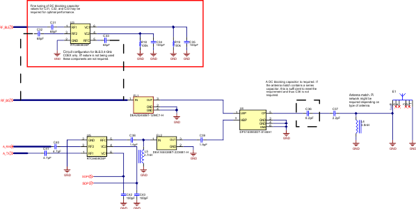
Figure 10-7 shows the schematic of the engine area for the CC3135 device in the wide-voltage mode of operation, with the corresponding bill of materials show in Table 10-1. Figure 10-8 provides the schematic for the RF implementation with and without BLE/2.4 GHz coexistence, with the corresponding bill of materials shown in Table 10-2. For a full operation reference design, see the CC3135 SimpleLink™ WI-Fi® BoosterPack™ Design Files.
 Figure 10-7 CC3135
Engine Area
Figure 10-7 CC3135
Engine AreaTable 10-1 Bill of Materials for CC3135
Engine Area
| Quantity | Designator | Value | Manufacturer | Part Number | Description |
|---|---|---|---|---|---|
| 2 | C1, C2 | 100 µF | Taiyo Yuden | LMK325ABJ107MMHT | CAP, CERM, 100 µF, 10 V, +/- 20%, X5R, AEC-Q200 Grade 3, 1210 |
| 3 | C3, C5, C6 | 4.7 µF | Taiyo Yuden | JMK105BC6475MV-F | CAP, CERM, 4.7 uF, 6.3 V, +/- 20%, X6S, 0402 |
| 3 | C4, C15, C25 | 0.6 pF | MuRata | GJM0335C1ER60BB01D | CAP, CERM, 0.6pF, 25 V, +/- 16%, C0G/NP0, 0201 |
| 1 | C7 | 0.5 pF | Murata | GJM0335C1ER50BB01D | CAP, CERM, 0.5 pF, 25 V, +/- 20%, C0G/NP0, 0201 |
| 6 | C8, C9, C10, C12, C21, C22 | 0.1 µF | Walsin | CL05B104KO5NNNC | CAP, CERM, 0.1 µF, 16 V, +/- 10%, X7R, 0402 |
| 1 | C26 | 0.01 µF | Walsin | 0402B103K500CT | CAP, CERM, 0.01 µF, 50 V, +/- 10%, X7R, 0402 |
| 3 | C11, C19, C24 | 10 µF | Taiyo Yuden | LMK107BC6106MA-T | CAP, CERM, 10 uF, 10 V, +/- 20%, X6S, 0603 |
| 1 | C13 | 0.2 pF | MuRata | GJM0335C1ER20BB01D | CAP, CERM, 0.2pF, 25 V, +/- 50%, C0G/NP0, 0201 |
| 2 | C14, C23 | 0.1 µF | Samsung Electro-Mechanics | CL03A104KP3NNNC | CAP, CERM, 0.1 uF, 10 V, +/- 10%, X5R, 0201 |
| 2 | C16, C17 | 22 µF | MuRata | GRM188C80G226ME15J | CAP, CERM, 22 uF, 4 V, +/- 20%, X6S, 0603 |
| 1 | C18 | 1 µF | Walsin | CL05A105MP5NNNC | CAP, CERM, 1 µF, 10 V, +/- 20%, X5R, 0402 |
| 2 | C27, C28 | 10 pF | Walsin | 0402N100J500CT | CAP, CERM, 10 pF, 50 V, +/- 5%, C0G/NP0, 0402 |
| 2 | C29, C30 | 6.2 pF | Walsin | 0402N6R2C500CT | CAP, CERM, 6.2 pF, 50 V, +/- 4%, C0G/NP0, 0402 |
| 3 | J1, J2, J3 | Wurth Elektronik | 61300311121 | Header, 2.54 mm, 3x1, Gold, TH | |
| 2 | L1, L3 | 2.2 µH | MuRata | LQM2MPN2R2NG0 | Inductor, Multilayer, Ferrite, 2.2 uH, 1.2 A, 0.11 ohm, SMD |
| 1 | L2 | 1 µH | MuRata | LQM2HPN1R0MG0L | Inductor, Multilayer, Ferrite, 1 uH, 1.6 A, 0.055 ohm, SMD |
| 1 | R1 | Vishay-Dale | CRCW040210K0JNED | RES, 10 k, 5%, 0.063 W, AEC-Q200 Grade 0, 0402 | |
| 10 | R2, R3, R4, R5, R6, R7, R11, R13, R14, R15 | 100k | Vishay-Dale | CRCW0402100KJNED | RES, 100 k, 5%, 0.063 W, AEC-Q200 Grade 0, 0402 |
| 1 | R8 | 270 | Vishay-Dale | CRCW0402270RJNED | RES, 270, 5%, 0.063 W, AEC-Q200 Grade 0, 0402 |
| 1 | R12 | 100k | Yageo America | RC0201JR-07100KL | RES, 100 k, 5%, 0.05 W, 0201 |
| 4 | R9, R10, R16, R17 | 69.8k | Vishay-Dale | CRCW040269K8FKED | RES, 69.8 k, 1%, 0.063 W, AEC-Q200 Grade 0, 0402 |
| 1 | U1 | Macronix International Co., LTD | MX25R3235FM1IL0 | Ultra low power, 32M-bit [x 1/x 2/x 4] CMOS MXSMIO (serial multi I/O) Flash memory, SOP-8 |
|
| 1 | U2 | Texas Instruments | CC3135RNMRGKR | SimpleLink Wi-Fi, Dual-Band Network Processor, RGK0064B (VQFN-64) |
|
| 1 | Y1 | Abracon Corporation | ABS07-32.768KHZ-9-T | Crystal, 32.768 kHz, 9PF, SMD | |
| 1 | Y2 | TXC Corporation | 8Y40072002 | Crystal, 40 MHz, 8 pF, SMD |
 Figure 10-8 CC3135 RF Schematic
Implementation With and Without Coexistence
Figure 10-8 CC3135 RF Schematic
Implementation With and Without CoexistenceNote:
The Following guidelines are recommended for implementation of the RF design:
- Ensure an RF path is designed with an impedance of 50 Ω
- Tuning of the antenna impedance π matching network is recommended after manufacturing of the PCB to account for PCB parasitics
- π or L matching and tuning may be required between cascaded passive components on the RF path
Table 10-2 Bill of Materials For CC3135
RF Section
| Quantity | Designator | Value | Manufacturer | Part Number | Description |
|---|---|---|---|---|---|
| 3 | C31(1), C32(1), C33(1) | 68 pF | Murata | GRM0335C1H680JA1D | CAP, CERM, 68 pF, 50 V, +/- 5%, C0G/NP0, 0201 |
| 4 | C34(1), C35(1), C42, C43 | 100 pF | Yageo | CC0201JRNPO8BN101 | CAP, CERM, 100 pF, 25 V, +/- 5%, C0G/NP0, 0201 |
| 1 | C36 | 8.2 pF | Walsin | 0402N8R2C500CT | CAP, CERM, 8.2 pF, 50 V, +/- 3%, C0G/NP0, 0402 |
| 1 | C37 | 2.2 pF | MuRata | GJM1555C1H2R2BB01D | CAP, CERM, 2.2 pF, 50 V, +/- 4.5%, C0G/NP0, 0402 |
| 1 | C38 | 1.6 pF | MuRata | GRM0335C1H1R6BA01D | CAP, CERM, 1.6 pF, 50 V, +/- 7%, C0G/NP0, 0201 |
| 1 | C39 | 1.9 pF | MuRata | GJM1555C1H1R9WB01D | CAP, CERM, 1.9 pF, 50 V, +/- 2.6%, C0G/NP0, 0402 |
| 2 | C40, C41 | 4.7 pF | MuRata | GRM0335C1H4R7BA01D | CAP, CERM, 4.7 pF, 50 V, +/- 3%, C0G/NP0, 0201 |
| 1 | E1 | Ethertronics | M830520 | WLAN ANTENNA 802.11, SMD | |
| 1 | FL1 | TDK | DEA202450BT-1294C1-H | Multilayer Chip Band Pass Filter For 2.4GHz W-LAN/Bluetooth, SMD | |
| 1 | FL2 | TDK | DEA165538BT-2236B1-H | Multilayer Band Pass Filter For 5GHz W-LAN/LTE-U | |
| 1 | L4 | 3.9 nH | MuRata | LQG15HS3N9S02D | Inductor, Multilayer, Air Core, 3.9 nH, 0.75 A, 0.14 ohm, SMD |
| 1 | L5 | 2.7 nH | MuRata | LQG15WH2N7C02D | Inductor, Multilayer, Air Core, 2.7 nH, 0.9 A, 0.07 ohm, AEC-Q200 Grade 1, SMD |
| 2 | R18(1), R19(1) | 100k | Vishay-Dale | CRCW0402100KJNED | RES, 100 k,
5%, 0.063 W, AEC-Q200 Grade 0, 0402 |
| 2 | U3(1), U5 | Richwave | RTC6608OSP | 0.03 GHz-6 GHz SPDT Switch | |
| 1 | U4 | TDK | DPX165950DT-8148A1 | Multilayer
Diplexer for 2.4 GHz W-LAN & Bluetooth / 5 GHz W-LAN |
(1) If the BLE/2.4 GHz Coexistence features is not used, these
components are not required.