JAJSHT5D February   2019  – May 2021 CC3135MOD

PRODUCTION DATA  

  1. 特長
  2. アプリケーション
  3. 概要
  4. 機能ブロック図
  5. Revision History
  6. Device Comparison
    1. 6.1 Related Products
  7. Terminal Configuration and Functions
    1. 7.1 CC3135MOD Pin Diagram
    2. 7.2 Pin Attributes
    3. 7.3 Signal Descriptions
      1.      12
    4. 7.4 Connections for Unused Pins
  8. Specifications
    1. 8.1  Absolute Maximum Ratings
    2. 8.2  ESD Ratings
    3. 8.3  Recommended Operating Conditions
    4. 8.4  Current Consumption Summary: 2.4 GHz RF Band
    5. 8.5  Current Consumption Summary: 5 GHz RF Band
    6. 8.6  TX Power Control for 2.4 GHz Band
    7. 8.7  TX Power Control for 5 GHz Band
    8. 8.8  Brownout and Blackout Conditions
    9. 8.9  Electrical Characteristics for DIO Pins
    10. 8.10 WLAN Receiver Characteristics
      1.      25
      2.      26
    11. 8.11 WLAN Transmitter Characteristics
      1.      28
      2.      29
    12. 8.12 BLE and WLAN Coexistence Requirements
    13. 8.13 Reset Requirement
    14. 8.14 Thermal Resistance Characteristics for MOB Package
    15. 8.15 Timing and Switching Characteristics
      1. 8.15.1 Power-Up Sequencing
      2. 8.15.2 Power-Down Sequencing
      3. 8.15.3 Device Reset
      4. 8.15.4 Wakeup From HIBERNATE Mode Timing
    16. 8.16 External Interfaces
      1. 8.16.1 SPI Host Interface
      2. 8.16.2 Host UART Interface
        1. 8.16.2.1 5-Wire UART Topology
        2. 8.16.2.2 4-Wire UART Topology
        3. 8.16.2.3 3-Wire UART Topology
      3. 8.16.3 External Flash Interface
  9. Detailed Description
    1. 9.1  Overview
    2. 9.2  Module Features
      1. 9.2.1 WLAN
      2. 9.2.2 Network Stack
        1. 9.2.2.1 Security
      3. 9.2.3 FIPS 140-2 Level 1 Certification
      4. 9.2.4 Host Interface and Driver
      5. 9.2.5 System
    3. 9.3  Power-Management Subsystem
      1. 9.3.1 VBAT Wide-Voltage Connection
    4. 9.4  Low-Power Operating Modes
      1. 9.4.1 Low-Power Deep Sleep
      2. 9.4.2 Hibernate
      3. 9.4.3 Shutdown
    5. 9.5  Restoring Factory Default Configuration
    6. 9.6  Hostless Mode
    7. 9.7  Device Certification and Qualification
      1. 9.7.1 FCC Certification and Statement
      2. 9.7.2 IC/ISED Certification Statement
      3. 9.7.3 ETSI/CE Certification
      4. 9.7.4 Japan MIC Certification
    8. 9.8  Module Markings
    9. 9.9  End Product Labeling
    10. 9.10 Manual Information to the End User
  10. 10Applications, Implementation, and Layout
    1. 10.1 Application Information
      1. 10.1.1 BLE/2.4 GHz Radio Coexistence
      2. 10.1.2 Antenna Selection
      3. 10.1.3 Typical Application
      4. 10.1.4 Power Supply Decoupling and Bulk Capacitors
      5. 10.1.5 Reset
      6. 10.1.6 Unused Pins
    2. 10.2 PCB Layout Guidelines
      1. 10.2.1 General Layout Recommendations
      2. 10.2.2 RF Layout Recommendations
      3. 10.2.3 Antenna Placement and Routing
      4. 10.2.4 Transmission Line Considerations
  11. 11Environmental Requirements and SMT Specifications
    1. 11.1 Temperature
      1. 11.1.1 PCB Bending
    2. 11.2 Handling Environment
      1. 11.2.1 Terminals
      2. 11.2.2 Falling
    3. 11.3 Storage Condition
      1. 11.3.1 Moisture Barrier Bag Before Opened
      2. 11.3.2 Moisture Barrier Bag Open
    4. 11.4 PCB Assembly Guide
      1. 11.4.1 PCB Land Pattern & Thermal Vias
      2. 11.4.2 SMT Assembly Recommendations
      3. 11.4.3 PCB Surface Finish Requirements
      4. 11.4.4 Solder Stencil
      5. 11.4.5 Package Placement
      6. 11.4.6 Solder Joint Inspection
      7. 11.4.7 Rework and Replacement
      8. 11.4.8 Solder Joint Voiding
    5. 11.5 Baking Conditions
    6. 11.6 Soldering and Reflow Condition
  12. 12Device and Documentation Support
    1. 12.1 Device Nomenclature
    2. 12.2 Development Tools and Software
    3. 12.3 Firmware Updates
    4. 12.4 Documentation Support
    5. 12.5 Trademarks
    6. 12.6 Electrostatic Discharge Caution
    7. 12.7 Export Control Notice
    8. 12.8 Glossary
  13. 13Mechanical, Packaging, and Orderable Information
    1. 13.1 Mechanical, Land, and Solder Paste Drawings
    2. 13.2 Package Option Addendum
      1. 13.2.1 Packaging Information
      2. 13.2.2 Tape and Reel Information
        1. 13.2.2.1 Tape Specifications

パッケージ・オプション

メカニカル・データ(パッケージ|ピン)
サーマルパッド・メカニカル・データ

Typical Application

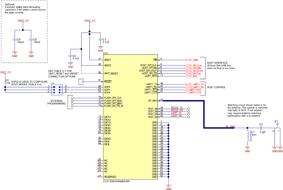
Figure 10-3 shows the typical application schematic using the CC3135MOD module.
GUID-8FC4EFD2-6790-4E6B-AFC0-DECAC7DF0AAF-low.gif
This is the reference schematic and not an actual board design. For a full operational reference design, see the CC3135MOD Hardware Design Files.
Figure 10-3 CC3135MOD Module Reference Schematic
Note:

The following guidelines are recommended for implementation of the RF design:

  • Ensure an RF path is designed with an impedance of 50 Ω
  • Tuning of the antenna impedance π matching network is recommended after manufacturing of the PCB to account for PCB parasitics
  • π or L matching and tuning may be required between cascaded passive components on the RF path

Table 10-1 lists the bill of materials for a typical application using the CC3135MOD module shown in Figure 10-3.

Table 10-1 Bill of Materials
QTYPART REFERENCEVALUEMANUFACTURERPART NUMBERDESCRIPTION
2C1, C20.1 uFMurataGRM155R61A104KA01DCapacitor, ceramic, 0.1 uF, 10 V, ±10%, X5R, 0402
1C33.3 pFMurataGJM1555C1H3R3BB01Capacitor, ceramic, 3.3 pF, 50 V, ±0.1pF, C0G/NP0, 0402
2C4, C5100 uFMurataLMK325ABJ107MMHTCapacitor, ceramic, 100 uF, 10 V, ±20%, X5R, AEC-Q200 Grade 3, 1210
1E12.4 GHz, 5 GHz AntEthertronicsM830520Antenna Bluetooth WLAN Zigbee®
1L13 nHMurataLQG15HS3N0S02DInductor, Unshielded, Multilayer, 3nH, 0.8 A, 0.125 Ω, SMD
1R110kVishay-DaleCRCW040210K0JNEDRES, 10 k, 5%, 0.063 W, AEC-Q200 Grade 0, 0402
1CC1CC3135MODTexas InstrumentsCC3135MODRNMMOBRSimpleLink™ Certified Wi-Fi® Dual-Band Network Processor Internet-of-Things Module Solution for MCU Applications, MOB0063A