JAJSOR2L August 1998 – September 2023 CD4051B , CD4052B , CD4053B
PRODUCTION DATA
- 1
- 1 特長
- 2 アプリケーション
- 3 概要
- 4 Revision History
- 5 Pin Configuration and Functions
- 6 Specifications
- 7 Parameter Measurement Information
- 8 Detailed Description
- 9 Application and Implementation
- 10Device and Documentation Support
- 11Mechanical, Packaging, and Orderable Information
パッケージ・オプション
メカニカル・データ(パッケージ|ピン)
サーマルパッド・メカニカル・データ
発注情報
7 Parameter Measurement Information
 Figure 7-1 Typical
Bias Voltages
Figure 7-1 Typical
Bias VoltagesNote:
The ADDRESS (digital-control
inputs) and INHIBIT logic levels are: 0 = VSS
and 1 = VDD. The analog signal
(through the TG) may swing from VEE to VDD.
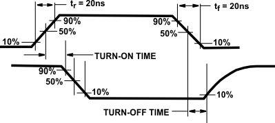 Figure 7-2 Waveforms, Channel Being Turned ON (RL = 1 kΩ)
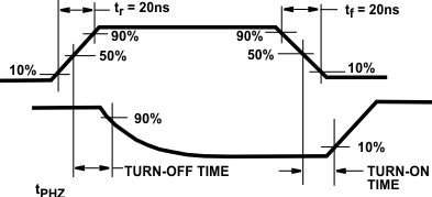 Figure 7-3 Waveforms, Channel Being Turned OFF (RL = 1 kΩ)
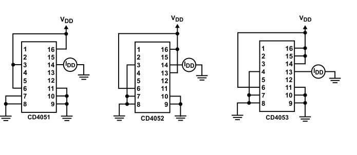 Figure 7-4 OFF
Channel Leakage Current – Any Channel OFF
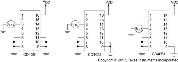 Figure 7-5 On Channel Leakage Current –
Any Channel On
 Figure 7-6 OFF
Channel Leakage Current – All Channels OFF
 Figure 7-7 Propagation Delay – Address Input to Signal Output
 Figure 7-8 Propagation Delay – Inhibit Input to Signal Output
 Figure 7-9 Input
Voltage Test Circuits (Noise Immunity)
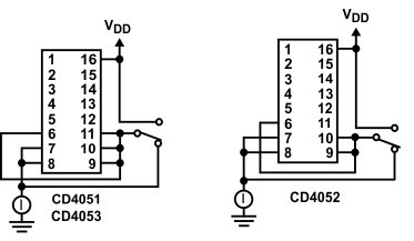 Figure 7-10 Quiescent Device Current
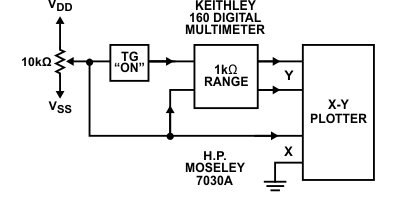 Figure 7-11 Channel ON Resistance Measurement Circuit
 Figure 7-12 Input
Current
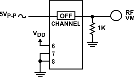 Figure 7-13 Feed-Through (All Types)
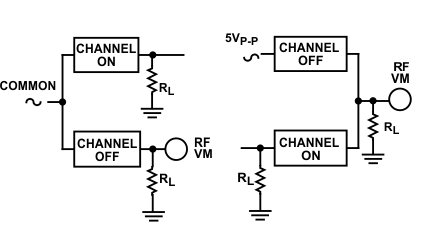 Figure 7-14 Crosstalk Between Any Two Channels (All Types)
 Figure 7-15 Crosstalk
Between Duals or Triplets (CD4052B,
CD4053B)
Special
Considerations: In applications where separate power sources are used to
drive VDD and the signal inputs, the VDD current
capability should exceed VDD/RL (RL = effective
external load). This provision avoids permanent current flow or clamp action on
the VDD supply when power is applied or removed from the CD4051B,
CD4052B or CD4053B.
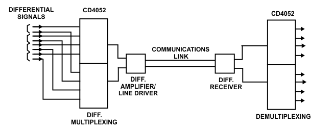
Figure 7-16 Typical
Time-Division Application of the CD4052B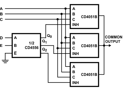 Figure 7-17 24-to-1
MUX Addressing