DATA SHEET
CD74HC4051-EP Analog Multiplexer and Demultiplexer
1 Features
-
Controlled Baseline
- One Assembly and Test Site, One Fabrication Site
- Extended Temperature Performance of –55°C to 125°C
- Enhanced Diminishing Manufacturing Sources (DMS) Support
- Enhanced Product Change Notification
- Qualification Pedigree(1)
- Wide Analog Input Voltage Range of ±5 V Max
- Low ON-Resistance
- 70 Ω Typical (VCC – VEE = 4.5 V)
- 40 Ω Typical (VCC – VEE = 9 V)
- Low Crosstalk Between Switches
- Fast Switching and Propagation Speeds
- Break-Before-Make Switching
- Operation Control Voltage = 2 V to 6 V
- Switch Voltage = 0 V to 10 V
- High Noise Immunity NIL = 30%, NIH = 30% of VCC, VCC = 5 V (1)
(1) Component qualification in accordance with JEDEC and industry standards to ensure reliable operation over an extended Accelerated Stress Test (HAST) or biased 85/85, temperature cycle, autoclave or unbiased HAST, electromigration, bond intermetallic life, and mold compound life. Such qualification testing should not be viewed as justifying use of this component beyond specified performance and environmental limits.
2 Applications
Supports Defense and Aerospace Applications
3 Description
The CD74HC4051-EP is a digitally controlled analog switch that uses silicon gate CMOS technology to achieve operating speeds similar to LSTTL, with the low power consumption of standard CMOS integrated circuits.
This analog multiplexer and demultiplexer controls analog voltages that may vary across the voltage supply range (that is, VCC to VEE). These bidirectional switches allow the use of any analog input as an output and vice versa. The switches have low ON-resistance and low OFF leakages. In addition, the device has an enable control (E) that, when high, disables all switches to their OFF state.
Device Information(1)
| PART NUMBER | PACKAGE | BODY SIZE (NOM) |
|---|---|---|
| CD74HC4051-EP | SOIC (16) | 4.00 mm × 10.00 mm |
- For all available packages, see the orderable addendum at the end of the data sheet.
Functional Block Diagram

4 Revision History
Changes from * Revision (September 2002) to A Revision
- Added ESD Ratings table, Feature Description section, Device Functional Modes, Application and Implementation section, Power Supply Recommendations section, Layout section, Device and Documentation Support section, and Mechanical, Packaging, and Orderable Information section. Go
5 Pin Configuration And Functions
D Package
16-Pin SOIC
Top View
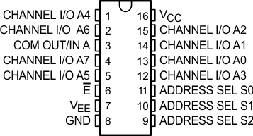
Pin Functions
| PIN | I/O | DESCRIPTION | |
|---|---|---|---|
| NAME | NO. | ||
| A4 | 1 | I/O | Channel 4 input / output |
| A6 | 2 | I/O | Channel 6 Input / output |
| A | 3 | I/O | COM OUT/ IN |
| A7 | 4 | I/O | Channel 7 Input / Output |
| A5 | 5 | I/O | Channel 5 Input / Output |
| Ebar | 6 | I | Enable input |
| VEE | 7 | I | Power input level for incoming Channel |
| GND | 8 | I | Power GND |
| VCC | 9 | I | Power input level for outgoing Channel |
| A2 | 10 | I/O | Channel 2 Input / Output |
| A1 | 11 | I/O | Channel 1 Input / Output |
| A0 | 12 | I/O | Channel 0 Input / Output |
| A3 | 13 | I/O | Channel 3 Input / Output |
| S0 | 14 | I | Address Select Input 0 |
| S1 | 15 | I | Address Select Input 1 |
| S2 | 15 | I | Address Select Input 2 |
6 Specifications
6.1 Absolute Maximum Ratings
over operating free-air temperature range (unless otherwise noted) (1)| MIN | MAX | UNIT | ||
|---|---|---|---|---|
| VCC – VEE(2) | Supply voltage | –0.5 | 10.5 | V |
| VCC | –0.5 | 7 | ||
| VEE | 0.5 | –7 | ||
| IIK | Input clamp current (VI < –0.5 V or VI > VCC + 0.5 V) | –20 | 20 | mA |
| IOK | Output clamp current (VO < VEE – 0.5 V or VO > VCC + 0.5 V) | –20 | 20 | mA |
| Switch current (VI > VEE – 0.5 V or VI < VCC + 0.5 V) | –25 | 25 | mA | |
| Continuous current through VCC or GND | –50 | 50 | mA | |
| IEE | VEE current | 0 | 20 | mA |
| θJA | Package thermal impedance(3) | 73 | °C/W | |
| TJ | Maximum junction temperature | 150 | °C | |
| Tstg | Storage temperature | –65 | 150 | °C |
(1) Stresses beyond those listed under Absolute Maximum Ratings may cause permanent damage to the device. These are stress ratings only, which do not imply functional operation of the device at these or any other conditions beyond those indicated under Recommended Operating Conditions. Exposure to absolute-maximum-rated conditions for extended periods may affect device reliability.
(2) All voltages referenced to GND unless otherwise specified.
(3) The package thermal impedance is calculated in accordance with JESD 51-7.
6.2 ESD Ratings
| VALUE | UNIT | ||||
|---|---|---|---|---|---|
| V(ESD) | Electrostatic discharge | Human body model (HBM), per ANSI/ESDA/JEDEC JS-001, all pins(1) | ±2000 | V | |
| Charged device model (CDM), per JEDEC specification JESD22-C101, all pins(2) | ±500 | ||||
(1) JEDEC document JEP155 states that 500-V HBM allows safe manufacturing with a standard ESD control process.
(2) JEDEC document JEP157 states that 250-V CDM allows safe manufacturing with a standard ESD control process.
6.3 Recommended Operating Conditions(1)
over operating free-air temperature range (unless otherwise noted)| MIN | NOM | MAX | UNIT | |||
|---|---|---|---|---|---|---|
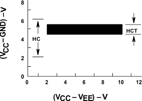
| VCC | Supply voltage(2) | 2 6 | 6 | V | ||
| Supply voltage, VCC – VEE (see Figure 4) | 2 10 | 10 | V | |||
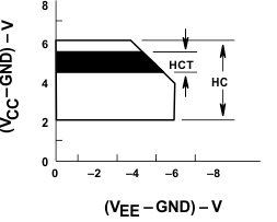
| VEE | Supply voltage, (see (2) and Figure 5) | 0 –6 | –6 | V | ||
| VIH | High-level input voltage | VCC = 2 V | 1.5 | V | ||
| VCC = 4.5 V | 3.15 | |||||
| VCC = 6 V | 4.2 | |||||
| VIL | Low-level input voltage | VCC = 2 V | 0.5 | V | ||
| VCC = 4.5 V | 1.35 | |||||
| VCC = 6 V | 1.8 | |||||
| VI | Input control voltage | 0 | VCC | V | ||
| VIS | Analog switch I/O voltage | VEE | VCC | V | ||
| tt | Input transition (rise and fall) time | VCC = 2 V | 0 | 1000 | ns | |
| VCC = 4.5 V | 0 | 500 | ||||
| VCC = 6 V | 0 | 400 | ||||
| TA | Operating free-air temperature | –55 | 125 | °C | ||
| Cpd | Power dissipation capacitance(3) | 50 | pF | |||
(1) All unused inputs of the device must be held at VCC or GND to ensure proper device operation. Refer to the TI application report, Implications of Slow or Floating CMOS Inputs, SCBA004.
(2) In certain applications, the external load resistor current may include both VCC and signal-line components. To avoid drawing VCC current when switch current flows into the transmission gate inputs, the voltage drop across the bidirectional switch must not exceed 0.6 V (calculated from ron values shown in Electrical Characteristics table). No VCC current flows through RL if the switch current flows into the COM OUT/IN A terminal.
(3) Cpd is used to determine the dynamic power consumption, per package.
PD = Cpd VCC2 fI + Σ (CL + CS) VCC2 fO
fO = output frequency
fI = input frequency
CL = output load capacitance
CS = switch capacitance
VCC = supply voltage
PD = Cpd VCC2 fI + Σ (CL + CS) VCC2 fO
fO = output frequency
fI = input frequency
CL = output load capacitance
CS = switch capacitance
VCC = supply voltage
6.4 Thermal Information
| THERMAL METRIC(1) | CD74HC4051-EP | UNIT | |
|---|---|---|---|
| D (SOIC) | |||
| 16 PINS | |||
| RθJA | Junction-to-ambient thermal resistance | 81.7 | °C/W |
| RθJC(top) | Junction-to-case (top) thermal resistance | 43.1 | |
| RθJB | Junction-to-board thermal resistance | 39.2 | |
| ψJT | Junction-to-top characterization parameter | 10.7 | |
| ψJB | Junction-to-board characterization parameter | 38.9 | |
(1) For more information about traditional and new thermal metrics, see the IC Package Thermal Metrics application report, SPRA953.
6.5 Electrical Characteristics
over operating free-air temperature range (unless otherwise noted)| PARAMETER | TEST CONDITIONS | VEE | VCC | TA = 25°C | TA = –55°C to 125°C | UNIT | |||||
|---|---|---|---|---|---|---|---|---|---|---|---|
| MIN | TYP | MAX | MIN | TYP | MAX | ||||||
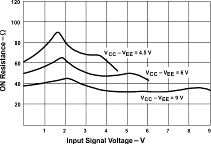
| ron | IO = 1 mA, VI = VIH or VIL, See Figure 1 |
VIS = VCC or VEE | 0 V | 4.5 V | 70 | 160 | 240 | Ω | |||
| 0 V | 6 V | 60 | 140 | 210 | |||||||
| –4.5 V | 4.5 V | 40 | 120 | 180 | |||||||
| VIS = VCC to VEE | 0 V | 4.5 V | 90 | 180 | 270 | ||||||
| 0 V | 6 V | 80 | 160 | 240 | |||||||
| –4.5 V | 4.5 V | 45 | 130 | 195 | |||||||
| ∆ron | Between any two channels | 0 V | 4.5 V | 10 | Ω | ||||||
| 0 V | 6 V | 8.5 | |||||||||
| –4.5 V | 4.5 V | 5 | |||||||||
| IIZ | For switch OFF: When VIS = VCC, VOS = VEE; When VIS = VEE, VOS = VCC For switch ON: All applicable combinations of VIS and VOS voltage levels, VI = VIH or VIL |
0 V | 6 V | ±0.2 | ±2 | µA | |||||
| –5 V | 5 V | ±0.4 | ±4 | ||||||||
| IIL | VI = VCC or GND | 0 V | 6 V | ±0.1 | ±1 | µA | |||||
| ICC | IO = 0, VI = VCC or GND | When VIS = VEE, VOS = VCC | 0 V | 6 V | 8 | 160 | µA | ||||
| When VIS = VCC, VOS = VEE | –5 V | 5 V | 16 | 320 | |||||||
6.6 Analog Channel Characteristics
TA = 25°C| PARAMETER | TEST CONDITIONS | VEE | VCC | MIN | TYP | MAX | UNIT | |
|---|---|---|---|---|---|---|---|---|
| CI | Switch input capacitance | 5 | pF | |||||
| CCOM | Common output capacitance | 25 | pF | |||||
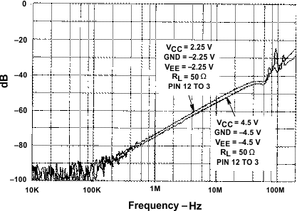
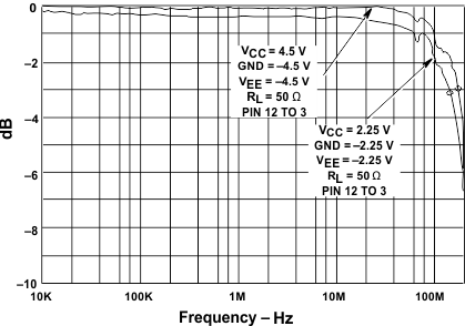
| fmax | Minimum switch frequency response at –3 dB | See Figure 6, Figure 2, and (1)(2) | –2.25 V | 2.25 V | 145 | MHz | ||
| –4.5 V | 4.5 V | 180 | ||||||
| Sine-wave distortion | See Figure 7 | –2.25 V | 2.25 V | 0.03% | ||||
| –4.5 V | 4.5 V | 0.018% | ||||||
| Switch OFF signal feedthrough | See Figure 8, Figure 3 and (2)(3) | –2.25 V | 2.25 V | –73 | dB | |||
| –4.5 V | 4.5 V | –75 | ||||||
(1) Adjust input voltage to obtain 0 dBm at VOS for fIN = 1 MHz.
(2) VIS is centered at (VCC – VEE)/2.
(3) Adjust input for 0 dBm
6.7 Switching Characteristics
over recommended operating free-air temperature range (unless otherwise noted) (see Figure 9)| PARAMETER | FROM (INPUT) |
TO (OUTPUT) |
LOAD CAPACITANCE |
VEE | VCC | TA = 25°C | TA = –55°C TO 125°C | UNIT | ||||
|---|---|---|---|---|---|---|---|---|---|---|---|---|
| MIN | TYP | MAX | MIN | TYP | MAX | |||||||
| tpd | IN | OUT | CL = 15 pF | 5 V | 4 | ns | ||||||
| CL = 50 pF | 0 V | 2 V | 60 | 90 | ||||||||
| 4.5 V | 12 | 18 | ||||||||||
| 6 V | 10 | 15 | ||||||||||
| –4.5 V | 4.5 V | 8 | 12 | |||||||||
| CL = 15 pF | 5 V | 19 | ns | |||||||||
| ten | ADDRESS SEL or E | OUT | CL = 50 pF | 0 V | 2 V | 225 | 340 | |||||
| 4.5 V | 45 | 68 | ||||||||||
| 6 V | 38 | 57 | ||||||||||
| –4.5 V | 4.5 V | 32 | 48 | |||||||||
| tdis | ADDRESS SEL or E | OUT | CL = 15 pF | 5 V | 19 | ns | ||||||
| CL = 50 pF | 0 V | 2 V | 225 | 340 | ||||||||
| 4.5 V | 45 | 68 | ||||||||||
| 6 V | 38 | 57 | ||||||||||
| –4.5 V | 4.5 V | 32 | 48 | |||||||||
| CI | Control | CL = 50 pF | 10 | 10 | pF | |||||||
6.8 Typical Characteristics
6.8.1 Recommended Operating Area as a Function of Supply Voltages