SCLS464A September 2002 – January 2015 CD74HC4051-EP
PRODUCTION DATA.
- 1 Features
- 2 Applications
- 3 Description
- 4 Revision History
- 5 Pin Configuration And Functions
- 6 Specifications
- 7 Parameter Measurement Information
- 8 Detailed Description
- 9 Application and Implementation
- 10Power Supply Recommendations
- 11Layout
- 12Device And Documentation Support
- 13Mechanical, Packaging, and Orderable Information
パッケージ・オプション
デバイスごとのパッケージ図は、PDF版データシートをご参照ください。
メカニカル・データ(パッケージ|ピン)
- D|16
サーマルパッド・メカニカル・データ
発注情報
9 Application and Implementation
NOTE
Information in the following applications sections is not part of the TI component specification, and TI does not warrant its accuracy or completeness. TI’s customers are responsible for determining suitability of components for their purposes. Customers should validate and test their design implementation to confirm system functionality.
9.1 Application Information
9.1.1 TTL-to-HC Interface
TTL output voltages and HC input voltages are incompatible, especially between the TTL high-level output voltage (VOH) and the HC high-level input voltage (VIH). This problem can be solved in two different ways. The first solution is to provide pullup resistors at the TTL outputs to ensure an adequate high-level TTL output voltage. A alternative method requires the use of level shifters.
9.2 Typical Application
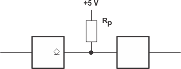 Figure 11. Typical Application Schematic TTL-to-HC Interface Using Open-Collector Output.
9.2.1 Design Requirements
Interfacing TTL open-collector outputs to HC-CMOS inputs requires design of pullup circuit balanced with drive capability to achieve timing and VOL-HC input specifications. Similar technique can be applied when using open-drain outputs.
9.2.2 Detailed Design Procedure
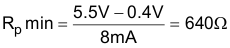
Using pullup resistors to accommodate TTL output signals to interface with HC input circuits (see Figure 11), the design engineer must choose the resistance that is appropriate for the application. The minimum value of the resistor is determined by the maximum current IOL that a TTL circuit can supply at the low-level output (VOL).
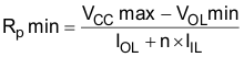
where
- n is the number of HC inputs to be driven
- IIL is their input current
IIL, having a value of only a few nanoamperes, is negligible in all calculations.
In the case of a SN74ALS03, Equation 2 defines Rpmin:
To calculate the upper limit of this resistor, a sufficient VIH high level must be ensured.
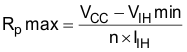
In this situation, the input current of HC devices is negligible and very high values also are obtained.
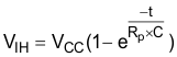
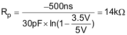
When calculating the maximum allowable resistance, it is important to ensure that the maximum allowable rise time (tr = 500 ns) at the HC input is not exceeded. Equation 4 then applies:
where
- C is the total load capacitance in the circuit
C is composed of the output capacitance of the driving gate (approximately 10 pF), the total input capacitances of gates to be driven (approximately 5 pF each), and the line capacitance (approximately 1 pF/cm). The actual value is calculated by solving the equation for Rp:
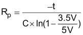
Assuming the total capacitance, C, is 30 pF, the maximum resistor is:
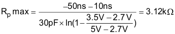
Faster rise times result in lower impedance and more power consumption. The previous calculation is based on the assumption that the driving gate has an open collector. Conditions become more satisfactory, however, when a gate with totem-pole output (that is, SN74ALS00) is used. In that case, the gate output provides the voltage to be brought up to the value VOH = 2.7 V in less than 10 ns (the rise time of the TTL signal). The pullup resistor only has to pull the level to 3.5 V within the desired time. According to the previous formula, and with a required rise time of tr = 50 ns, the resistor is defined by Equation 7:
The upper limiting value of the resistor is primarily dictated by the rise time required. The larger the resistance, the longer the rise times and propagation delay times. Reducing the resistance increases speed and power dissipation.
The other method of accommodating TTL signals to HC circuits is accomplished with special level shifters. This solution is not recommended because the level shifter itself has no inherent logic functions and increases component and space requirements.
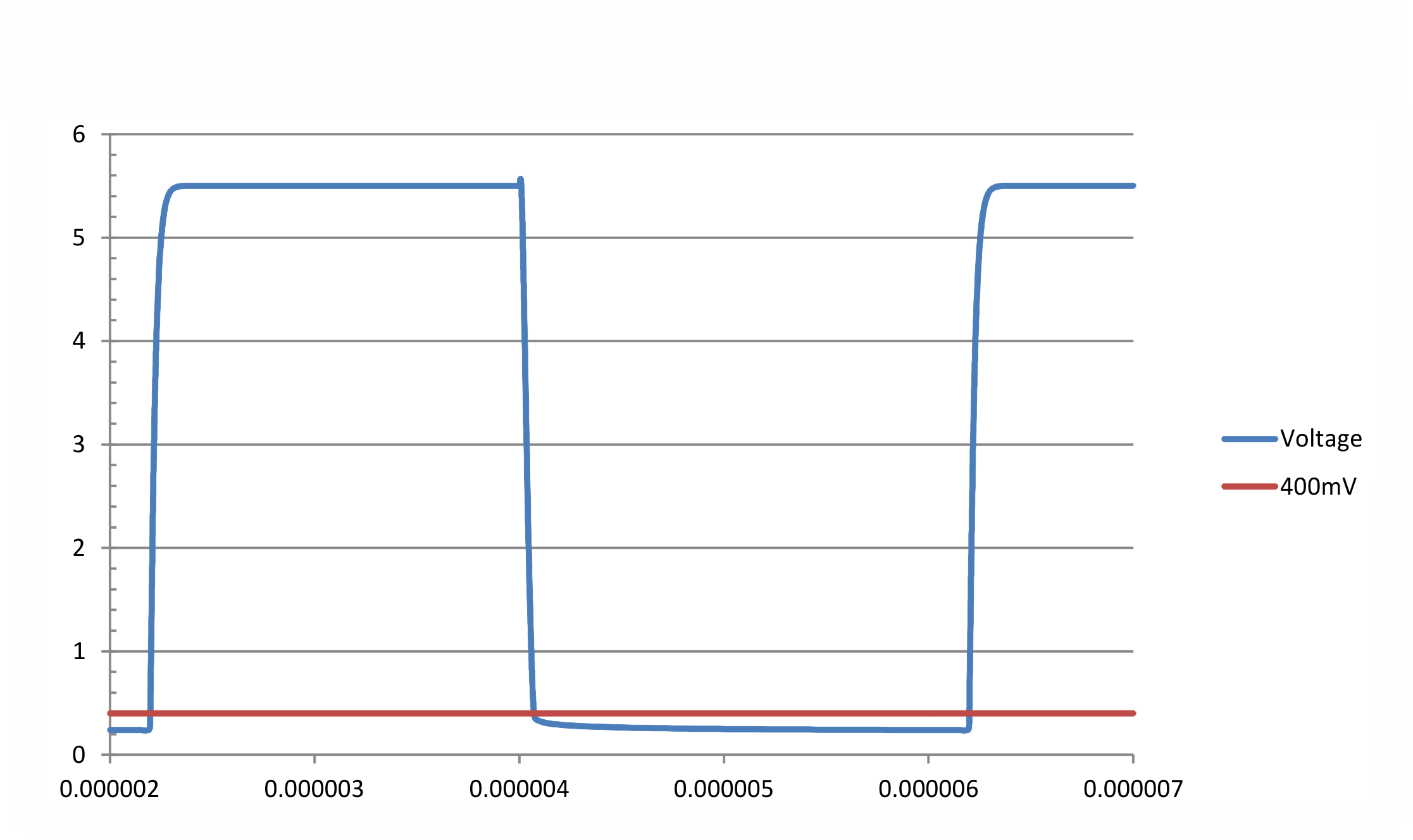
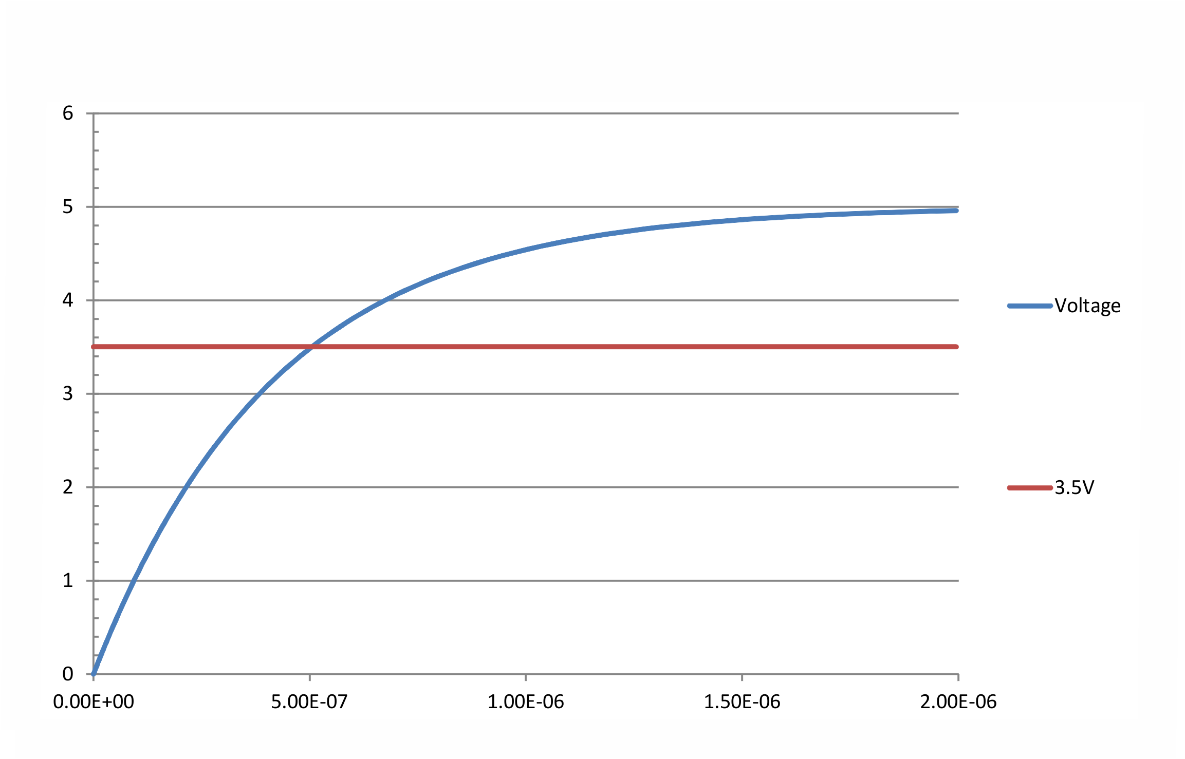
9.2.3 Application Curves