SCLS464A September 2002 – January 2015 CD74HC4051-EP
PRODUCTION DATA.
- 1 Features
- 2 Applications
- 3 Description
- 4 Revision History
- 5 Pin Configuration And Functions
- 6 Specifications
- 7 Parameter Measurement Information
- 8 Detailed Description
- 9 Application and Implementation
- 10Power Supply Recommendations
- 11Layout
- 12Device And Documentation Support
- 13Mechanical, Packaging, and Orderable Information
パッケージ・オプション
デバイスごとのパッケージ図は、PDF版データシートをご参照ください。
メカニカル・データ(パッケージ|ピン)
- D|16
サーマルパッド・メカニカル・データ
発注情報
5 Pin Configuration And Functions
D Package
16-Pin SOIC
Top View
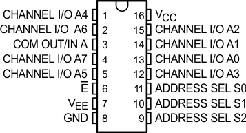
Pin Functions
| PIN | I/O | DESCRIPTION | |
|---|---|---|---|
| NAME | NO. | ||
| A4 | 1 | I/O | Channel 4 input / output |
| A6 | 2 | I/O | Channel 6 Input / output |
| A | 3 | I/O | COM OUT/ IN |
| A7 | 4 | I/O | Channel 7 Input / Output |
| A5 | 5 | I/O | Channel 5 Input / Output |
| Ebar | 6 | I | Enable input |
| VEE | 7 | I | Power input level for incoming Channel |
| GND | 8 | I | Power GND |
| VCC | 9 | I | Power input level for outgoing Channel |
| A2 | 10 | I/O | Channel 2 Input / Output |
| A1 | 11 | I/O | Channel 1 Input / Output |
| A0 | 12 | I/O | Channel 0 Input / Output |
| A3 | 13 | I/O | Channel 3 Input / Output |
| S0 | 14 | I | Address Select Input 0 |
| S1 | 15 | I | Address Select Input 1 |
| S2 | 15 | I | Address Select Input 2 |