JAJSG05H November   2009  – October 2024 CDC3RL02

PRODUCTION DATA  

  1.   1
  2. 特長
  3. アプリケーション
  4. 概要
  5. Device Comparison
  6. Pin Configuration and Functions
  7. Specifications
    1. 6.1 Absolute Maximum Ratings
    2. 6.2 ESD Ratings
    3. 6.3 Recommended Operating Conditions
    4. 6.4 Thermal Information
    5. 6.5 Electrical Characteristics
    6. 6.6 Typical Characteristics
  8. Detailed Description
    1. 7.1 Overview
    2. 7.2 Functional Block Diagram
    3. 7.3 Feature Description
      1. 7.3.1 Low Additive Noise
      2. 7.3.2 Regulated 1.8V Externally Available I/O Supply
      3. 7.3.3 Ultra-Small 8-bump YFP 0.4mm Pitch WCSP Package
    4. 7.4 Device Functional Modes
  9. Application and Implementation
    1. 8.1 Application Information
      1. 8.1.1 Input Clock Squarer
      2. 8.1.2 Output Stage
      3. 8.1.3 LDO
    2. 8.2 Typical Application
      1. 8.2.1 Design Requirements
      2. 8.2.2 Detailed Design Procedure
      3. 8.2.3 Application Curve
    3. 8.3 Power Supply Recommendations
    4. 8.4 Layout
      1. 8.4.1 Layout Guidelines
      2. 8.4.2 Layout Example
  10. Device and Documentation Support
    1. 9.1 Documentation Support
      1. 9.1.1 Related Documentation
    2. 9.2 ドキュメントの更新通知を受け取る方法
    3. 9.3 サポート・リソース
    4. 9.4 Trademarks
    5. 9.5 静電気放電に関する注意事項
    6. 9.6 用語集
  11. 10Revision History
  12. 11Mechanical, Packaging, and Orderable Information

パッケージ・オプション

メカニカル・データ(パッケージ|ピン)
サーマルパッド・メカニカル・データ
発注情報

Typical Application

The CDC3RL02 is designed for use in mobile applications as shown in Figure 8-2. In this example, a single low noise TCXO system clock source is buffered to drive a mobile GPS receiver and WLAN transceiver. Each peripheral independently requests an active clock by asserting a single clock request line (CLK_REQ_1 or CLK_REQ_2). When both clock request lines are inactive, the CDC3RL02 enters a low current shutdown mode. In this mode, the LDO output, CLK_OUT_1, and CLK_OUT_2 are pulled to GND and the TCXO is not powered.
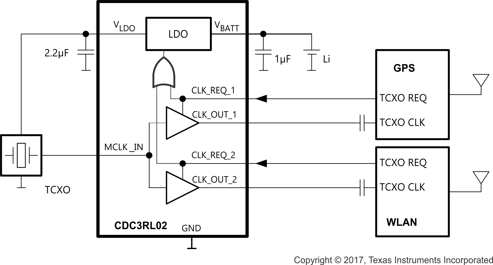
CDC3RL02 Mobile ApplicationFigure 8-2 Mobile Application

When either peripheral requests the clock, the CDC3RL02 enables the LDO and powers the TCXO. The TCXO output (square wave, sine wave, or clipped sine wave) is converted to a square wave and buffered to the requested output.