JAJSTU7H August 2007 – July 2024 CDCE937 , CDCEL937
PRODUCTION DATA
- 1
- 1 特長
- 2 アプリケーション
- 3 概要
- 4 Pin Configuration and Functions
- 5 Specifications
- 6 Parameter Measurement Information
- 7 Detailed Description
- 8 Register Maps
- 9 Application and Implementation
- 10Power Supply Recommendations
- 11Layout
- 12Device and Documentation Support
- 13Revision History
- 14Mechanical, Packaging, and Orderable Information
7.3.2 Default Device Setting
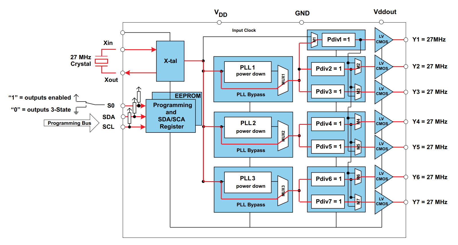
The internal EEPROM of CDCEx937 is preconfigured as shown in Figure 7-1. (The input frequency is passed through to the output as a default.) This allows the device to operate in default mode without the extra production step of programming. The default setting appears after power is supplied or after power-down or power-up sequence until the settings are reprogrammed by the user to a different application configuration. A new register setting is programmed through the serial SDA/SCL Interface
 Figure 7-1 Default Device Setting
Table 7-4 shows the factory default setting for the Control Terminal Register (external control pins). In normal operation, all 8 register settings are available, but in the default configuration only the first two settings (0 and 1) can be selected with S0, as S1 and S2 configured as programming pins in default mode.
| Y1 | PLL1 SETTINGS | PLL2 SETTINGS | PLL3 SETTINGS | |||||||||||||||||||
|---|---|---|---|---|---|---|---|---|---|---|---|---|---|---|---|---|---|---|---|---|---|---|
| EXTERNAL CONTROL PINS |
OUTPUT SELECTION |
FREQUENCY SELECTION |
SSC SELECTION |
OUTPUT SELECTION |
FREQUENCY SELECTION |
SSC SELECTION |
OUTPUT SELECTION |
FREQUENCY SELECTION |
SSC SELECTION |
OUTPUT SELECTION |
||||||||||||
| S2 | S1 | S0 | Y1 | FS1 | SSC1 | Y2Y3 | FS2 | SSC2 | Y4Y5 | FS3 | SSC3 | Y6Y7 | ||||||||||
| SCL (I2C) | SDA (I2C) | 0 | 3-state | fVCO1_0 | off | 3-state | fVCO2_0 | off | 3-state | fVCO3_0 | off | 3-state | ||||||||||
| SCL (I2C) | SDA (I2C) | 1 | enabled | fVCO1_0 | off | enabled | fVCO2_0 | off | enabled | fVCO3_0 | off | enabled | ||||||||||