SLAS564H August   2007  – July 2024 CDCE937 , CDCEL937

PRODUCTION DATA  

  1.   1
  2. Features
  3. Applications
  4. Description
  5. Pin Configuration and Functions
  6. Specifications
    1. 5.1 Absolute Maximum Ratings
    2. 5.2 ESD Ratings
    3. 5.3 Recommended Operating Conditions
    4. 5.4 Thermal Information
    5. 5.5 Electrical Characteristics
    6. 5.6 Timing Requirements: CLK_IN
    7. 5.7 Timing Requirements: SDA/SCL
    8. 5.8 EEPROM Specification
    9. 5.9 Typical Characteristics
  7. Parameter Measurement Information
  8. Detailed Description
    1. 7.1 Overview
    2. 7.2 Functional Block Diagram
    3. 7.3 Feature Description
      1. 7.3.1 Control Terminal Setting
      2. 7.3.2 Default Device Setting
      3. 7.3.3 SDA/SCL Serial Interface
      4. 7.3.4 Data Protocol
    4. 7.4 Device Functional Modes
      1. 7.4.1 SDA/SCL Hardware Interface
    5. 7.5 Programming
  9. Register Maps
    1. 8.1 SDA/SCL Configuration Registers
  10. Application and Implementation
    1. 9.1 Application Information
    2. 9.2 Typical Application
      1. 9.2.1 Design Requirements
      2. 9.2.2 Detailed Design Procedure
        1. 9.2.2.1 Spread Spectrum Clock (SSC)
        2. 9.2.2.2 PLL Frequency Planning
        3. 9.2.2.3 Crystal Oscillator Start-Up
        4. 9.2.2.4 Frequency Adjustment With Crystal Oscillator Pulling
        5. 9.2.2.5 Unused Inputs and Outputs
        6. 9.2.2.6 Switching Between XO and VCXO Mode
      3. 9.2.3 Application Curves
  11. 10Power Supply Recommendations
  12. 11Layout
    1. 11.1 Layout Guidelines
    2. 11.2 Layout Example
  13. 12Device and Documentation Support
    1. 12.1 Device Support
      1. 12.1.1 Third-Party Products Disclaimer
      2. 12.1.2 Development Support
    2. 12.2 Documentation Support
      1. 12.2.1 Related Documentation
    3. 12.3 Receiving Notification of Documentation Updates
    4. 12.4 Support Resources
    5. 12.5 Trademarks
    6. 12.6 Electrostatic Discharge Caution
    7. 12.7 Glossary
  14. 13Revision History
  15. 14Mechanical, Packaging, and Orderable Information

パッケージ・オプション

メカニカル・データ(パッケージ|ピン)
サーマルパッド・メカニカル・データ
発注情報

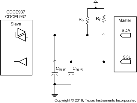
SDA/SCL Hardware Interface

Figure 7-3 shows how the CDCEx937 clock synthesizer is connected to the SDA/SCL serial interface bus. Multiple devices can be connected to the bus but the speed can require reduction (400 kHz is the maximum) if many devices are connected.

Note that the pullup resistors (RP) depends on the supply voltage, bus capacitance, and number of connected devices. The recommended pullup value is 4.7 kΩ. The pullup value must meet the minimum sink current of 3 mA at
VOLmax = 0.4 V for the output stages (for more details, see SMBus or I2C Bus specification).
CDCE937 CDCEL937 SDA/SCL Hardware InterfaceFigure 7-3 SDA/SCL Hardware Interface