SLAS564H August   2007  – July 2024 CDCE937 , CDCEL937

PRODUCTION DATA  

  1.   1
  2. Features
  3. Applications
  4. Description
  5. Pin Configuration and Functions
  6. Specifications
    1. 5.1 Absolute Maximum Ratings
    2. 5.2 ESD Ratings
    3. 5.3 Recommended Operating Conditions
    4. 5.4 Thermal Information
    5. 5.5 Electrical Characteristics
    6. 5.6 Timing Requirements: CLK_IN
    7. 5.7 Timing Requirements: SDA/SCL
    8. 5.8 EEPROM Specification
    9. 5.9 Typical Characteristics
  7. Parameter Measurement Information
  8. Detailed Description
    1. 7.1 Overview
    2. 7.2 Functional Block Diagram
    3. 7.3 Feature Description
      1. 7.3.1 Control Terminal Setting
      2. 7.3.2 Default Device Setting
      3. 7.3.3 SDA/SCL Serial Interface
      4. 7.3.4 Data Protocol
    4. 7.4 Device Functional Modes
      1. 7.4.1 SDA/SCL Hardware Interface
    5. 7.5 Programming
  9. Register Maps
    1. 8.1 SDA/SCL Configuration Registers
  10. Application and Implementation
    1. 9.1 Application Information
    2. 9.2 Typical Application
      1. 9.2.1 Design Requirements
      2. 9.2.2 Detailed Design Procedure
        1. 9.2.2.1 Spread Spectrum Clock (SSC)
        2. 9.2.2.2 PLL Frequency Planning
        3. 9.2.2.3 Crystal Oscillator Start-Up
        4. 9.2.2.4 Frequency Adjustment With Crystal Oscillator Pulling
        5. 9.2.2.5 Unused Inputs and Outputs
        6. 9.2.2.6 Switching Between XO and VCXO Mode
      3. 9.2.3 Application Curves
  11. 10Power Supply Recommendations
  12. 11Layout
    1. 11.1 Layout Guidelines
    2. 11.2 Layout Example
  13. 12Device and Documentation Support
    1. 12.1 Device Support
      1. 12.1.1 Third-Party Products Disclaimer
      2. 12.1.2 Development Support
    2. 12.2 Documentation Support
      1. 12.2.1 Related Documentation
    3. 12.3 Receiving Notification of Documentation Updates
    4. 12.4 Support Resources
    5. 12.5 Trademarks
    6. 12.6 Electrostatic Discharge Caution
    7. 12.7 Glossary
  14. 13Revision History
  15. 14Mechanical, Packaging, and Orderable Information

パッケージ・オプション

メカニカル・データ(パッケージ|ピン)
サーマルパッド・メカニカル・データ
発注情報

Crystal Oscillator Start-Up

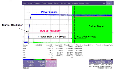
When the CDCEx937 is used as a crystal buffer, crystal oscillator start-up dominates the start-up time compared to the internal PLL lock time. Figure 9-4 shows the oscillator start-up sequence for a 27-MHz crystal input with an 8-pF load. The start-up time for the crystal is in the order of approximately 250 µs compared to approximately 10 µs of lock time. In general, lock time is an order of magnitude less compared to the crystal start-up time.
CDCE937 CDCEL937 Crystal Oscillator Start-Up vs PLL Lock TimeFigure 9-4 Crystal Oscillator Start-Up vs PLL Lock Time