SCAS759C April 2004 – July 2017 CDCM1802
PRODUCTION DATA.
- 1 Features
- 2 Applications
- 3 Description
- 4 Revision History
- 5 Pin Configuration and Functions
-
6 Specifications
- 6.1 Absolute Maximum Ratings
- 6.2 ESD Ratings
- 6.3 Recommended Operating Conditions
- 6.4 Thermal Information
- 6.5 Electrical Characteristics
- 6.6 Switching Characteristics
- 6.7 Jitter Characteristics
- 6.8 Supply Current Electrical Characteristics
- 6.9 Control Input Characteristics
- 6.10 Timing Requirements
- 6.11 Bias Voltage VBB
- 6.12 Typical Characteristics
- 7 Parameter Measurement Information
- 8 Detailed Description
- 9 Application and Implementation
- 10Power Supply Recommendations
- 11Layout
- 12Device and Documentation Support
- 13Mechanical, Packaging, and Orderable Information
パッケージ・オプション
メカニカル・データ(パッケージ|ピン)
- RGT|16
サーマルパッド・メカニカル・データ
- RGT|16
発注情報
11 Layout
11.1 Layout Guidelines
TI recommends taking special care of the PCB design for good thermal flow from the VQFN 16-pin package to the PCB. The current consumption of the CDCM1802 is fixed. JEDEC JESD51−7 specifies thermal conductivity for standard PCB boards.
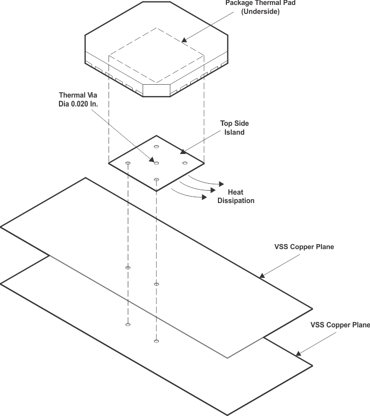
To ensure sufficient thermal flow, it is recommended to design with four thermal vias in applications.
See the SCBA017 and the SLUA271 application notes for further package-related information.
11.2 Layout Example
 Figure 21. Recommended Thermal Via Placement
11.3 Thermal Considerations
Table 2. Package Thermal Resistance
| PARAMETER | TEST CONDITIONS | MIN | TYP | MAX | UNIT | |
|---|---|---|---|---|---|---|
| RθJA | VQFN−16 package thermal resistance with thermal vias in PCB(1) | 4-layer JEDEC test board (JESD51−7) with four thermal vias of 22-mil diameter each, airflow = 0 ft/min | 48.4 | °C/W | ||
(1) It is recommended to provide four thermal vias to connect the thermal pad of the package effectively with the PCB and ensure a good heat sink.
| Example: | ||
| Calculation of the junction-lead temperature with a 4-layer JEDEC test board using four thermal vias: | ||
| TChassis = 85°C (temperature of the chassis) | ||
| Peffective = Imax × Vmax = 85 mA × 3.6 V = 306 mW (max power consumption inside the package) | ||
| ΔTJunction = RθJA × Peffective = 40.8°C/W × 306 mW = 12.48°C | ||
| TJunction = ΔTJunction + TChassis = 12.48°C + 85°C = 97.48°C (the maximum junction temperature of Tdie−max = 125°C is not violated) | ||