SCAS922A February 2012 – April 2016 CDCM9102
PRODUCTION DATA.
- 1 Features
- 2 Applications
- 3 Description
- 4 Revision History
- 5 Device Comparison Table
- 6 Pin Configuration and Functions
- 7 Specifications
- 8 Parameter Measurement Information
- 9 Detailed Description
- 10Application and Implementation
- 11Power Supply Recommendations
- 12Layout
- 13Device and Documentation Support
- 14Mechanical, Packaging, and Orderable Information
パッケージ・オプション
メカニカル・データ(パッケージ|ピン)
- RHB|32
サーマルパッド・メカニカル・データ
- RHB|32
発注情報
10 Application and Implementation
NOTE
Information in the following applications sections is not part of the TI component specification, and TI does not warrant its accuracy or completeness. TI’s customers are responsible for determining suitability of components for their purposes. Customers should validate and test their design implementation to confirm system functionality.
10.1 Application Information
10.1.1 Start-Up Time Estimation
The CDCM9102 contains a low-noise clock generator that calibrates to an optimal operating point at device power up. To ensure proper device operation, the oscillator must be stable before the low-noise clock generator calibration procedure. Quartz-based oscillators can take up to 2 ms to stabilize; therefore, TI recommends that the application ensure that the RESET pin is de-asserted at least 5 ms after the power supply has finished ramping. This can be accomplished by controlling the RESET pin directly, or by applying a 47-nF capacitor to ground on the RESET pin (this provides a delay because the RESET pin includes a 150-kΩ pullup resistor.
The CDCM9102 start-up time can be estimated based on parameters defined in Table 5 and graphically shown in Figure 10.
Table 5. CDCM9102 Start-Up Time Dependencies
| PARAMETER | DEFINITION | DESCRIPTION | FORMULA OR METHOD OF DETERMINATION |
|---|---|---|---|
| tREF | Reference clock period | The reciprocal of the applied reference frequency in seconds |  |
| tpul | Power-up time (low limit) | Power-supply rise time to low limit of power-on-reset trip point | Time required for power supply to ramp to 2.27 V |
| tpuh | Power-up time (high limit) | Power supply rise time to high limit of power-on-reset trip point | Time required for power supply to ramp to 2.64 V |
| trsu | Reference start-up time | After POR releases, the Colpitts oscillator is enabled. This start-up time is required for the oscillator to generate the requisite signal levels for the delay block to be clocked by the reference input. | 500 μs best case and 800 μs worst case (for a crystal input) |
| tdelay | Delay time | Internal delay time generated from the reference clock. This delay provides time for the reference oscillator to stabilize. | tdelay = 16,384 × tREF = 655 µs |
| tVCO_CAL | VCO calibration time | VCO calibration time generated from the reference clock. This process selects the operating point for the VCO based on the PLL settings. | tVCO_CAL = 550 × tREF = 22 µs |
| tPLL_LOCK | PLL lock time | Time requried for PLL to lock within ±10 ppm of fREF | The PLL settles in 12.5 μs |
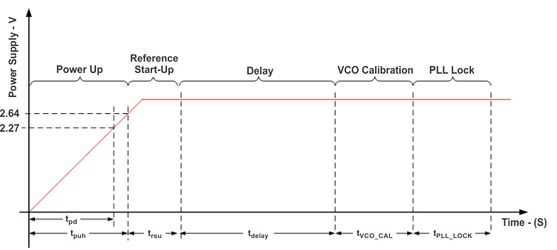 Figure 10. CDCM9102 Start-Up Time Dependencies
The CDCM9102 start-up time limits, tMAX and tMIN, can now be calculated with Equation 2 and Equation 3.
10.1.2 Output Termination
The CDCM9102 is a 3.3-V clock driver which has the following options for the output type: LVPECL, LVDS, and LVCMOS.
10.1.3 LVPECL Termination
The CDCM9102 is an open emitter for LVPECL outputs. Therefore, proper biasing and termination is required to ensure correct operation of the device and to optimize signal integrity. The proper termination for LVPECL is 50 Ω to (Vcc-2) V but this DC voltage is not readily available on a board. Thus a Thevenin’s equivalent circuit is worked out for the LVPECL termination in both direct-coupled (DC) and AC-coupled cases, as shown in Figure 11 and Figure 12. TI recommends placing all resistive components close to either the driver end or the receiver end. If the supply voltages of the driver and receiver are different, AC coupling is required.
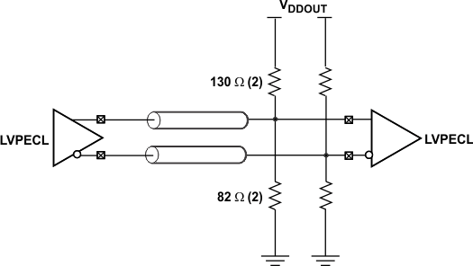 Figure 11. LVPECL Output Termination (DC-Coupled)
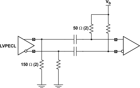 Figure 12. LVPECL Output Termination (AC-Coupled)
10.1.4 LVDS Termination
The proper LVDS termination for signal integrity over two 50-Ω lines is 100 Ω between the outputs on the receiver end. Either a direct-coupled (dc) termination or ac-coupled termination can be used for LVDS outputs, as shown in Figure 13 and Figure 14. TI recommends placing all resistive components close to either the driver end or the receiver end. If the supply voltages of the driver and receiver are different, AC coupling is required.
 Figure 13. LVDS Output Termination (DC Coupled)
 Figure 14. LVDS Output Termination (AC Coupling)
10.1.5 LVCMOS Termination
Series termination is a common method to maintain the signal integrity for LVCMOS drivers, if connected to a receiver with a high-impedance input. For series termination, a series resistor, Rs, is placed close to the driver, as shown in Figure 15. The sum of the driver impedance and Rs should be close to the transmission-line impedance, which is usually 50 Ω. Because the LVCMOS driver in the CDCM9102 has an impedance of 30 Ω, TI recommends Rs be 22 Ω to maintain proper signal integrity.
 Figure 15. LVCMOS Output Termination
10.1.6 PCI Express Applications
Texas Instruments offers a complete clock solution for PCI Express applications. The CDCUN1208LP can be used to fan out reference clock generated by the CDCM9102 as shown in Figure 16.
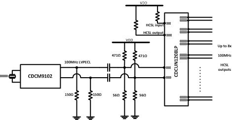 Figure 16. Clock Solution for PCIE Express Applications
10.2 Typical Application
 Figure 17. CDCM9102 Typical Application Example
10.2.1 Design Requirements
Consider a typical wired communications application, like a top-of-rack switch, which needs to clock PCI Express Gen 2 or 3 PHYs. For such asynchronous systems, the reference input can be a crystal. In such systems, the clocks are expected to be available upon power up without the need for any device-level programming. An example of clock input and output requirements is shown below:
- Clock Input:
- 25-MHz crystal
- Clock Outputs:
- 2× 100 MHz clock for PCI Express Gen 3 (8 GT/s), LVPECL
See Detailed Design Procedure for how to generate the required output frequencies for this application using the CDCM9102.
10.2.2 Detailed Design Procedure
Design of all aspects of the CDCM61004 is quite involved and software support is available to assist in part selection and phase noise simulation. This design procedure will give a quick outline of the process.
- Device Selection
- The first step is to calculate the VCO frequency given the required output frequency. The device must be able to produce the VCO frequency that can be divided down to the required output frequency.
- The WEBENCH Clock Architect Tool from TI will aid in the selection of the right device that meets the customer's output frequencies and format requirements.
- Device Configuration
- The WEBENCH Clock Architect Tool attempts to maximize the phase detector frequency, use smallest dividers, and maximizes PLL bandwidth.
10.2.2.1 Device Selection
Use the WEBENCH Clock Architect Tool. Enter the required frequencies and formats into the tool. To use this device, find a solution using the CDCM9102.
10.2.2.1.1 Calculation Using LCM
In this example, the valid VCO frequency for CDCM9102 is 1.8 GHz.
10.2.2.2 Device Configuration
For this example, when using the WEBENCH Clock Architect Tool, the reference would have been manually entered as 25 MHz according to input frequency requirements. Enter the desired output frequencies and click on Generate Solutions. Select CDCM9102 from the solution list.
From the simulation page of the WEBENCH Clock Architect Tool, it can be seen that to maximize phase detector frequencies, the N divider is set to 24 and prescaler divider is set to 3. This results in a VCO frequency of
1.8 GHz. The output divider is set to 6. At this point the design meets all input and output frequency requirements and simulate performance on the clock outputs. Figure 18 shows the typical phase noise plot of the 100 MHz LVPECL output.
10.2.3 Application Curve
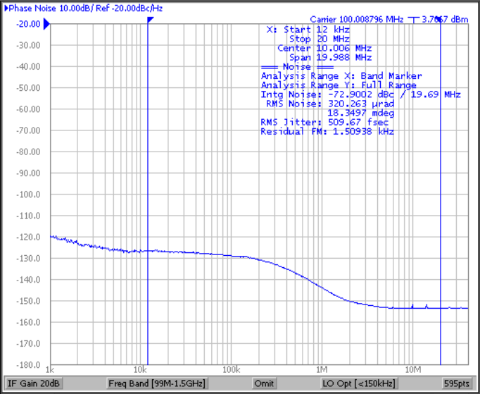 Figure 18. Typical Phase Noise Plot of 100 MHz LVPECL Output