JAJSS07A December 2014 – May 2024 CSD85301Q2
PRODUCTION DATA
4.2 Thermal Information
(TA = 25°C unless otherwise stated)
| THERMAL METRIC | MIN | TYP | MAX | UNIT | |
|---|---|---|---|---|---|
| RθJA | Junction-to-Ambient Thermal Resistance(1) | 70 | °C/W | ||
| Junction-to-Ambient Thermal Resistance(2) | 185 | ||||
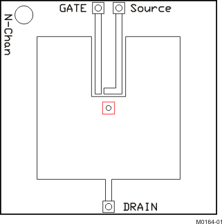
(1) Device mounted on FR4 material with 1 inch2 (6.45cm2),
2oz. (0.071mm thick) Cu.
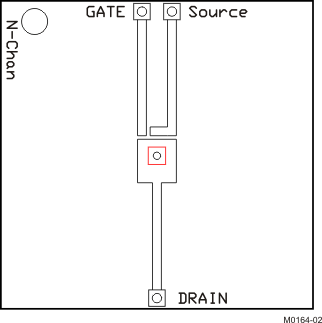
(2) Device mounted on FR4 material with minimum Cu mounting area.

| Max RθJA = 70 when mounted on
1 inch2 (6.45cm2) of 2oz. (0.071mm thick) Cu. | 
| Max RθJA = 185 when mounted on minimum pad
area of 2oz. (0.071mm thick) Cu. |