JAJSEY5 March   2018 CSD86336Q3D

PRODUCTION DATA.  

  1. 1特長
  2. 2アプリケーション
  3. 3概要
    1.     上面図
      1.      Device Images
  4. 4改訂履歴
  5. 5Specifications
    1. 5.1 Absolute Maximum Ratings
    2. 5.2 Recommended Operating Conditions
    3. 5.3 Thermal Information
    4. 5.4 Power Block Performance
    5. 5.5 Electrical Characteristics – Q1 Control FET
    6. 5.6 Electrical Characteristics – Q2 Sync FET
    7. 5.7 Typical Power Block Device Characteristics
    8. 5.8 Typical Power Block MOSFET Characteristics
  6. 6Application and Implementation
    1. 6.1 Application Information
      1. 6.1.1 Equivalent System Performance
    2. 6.2 Power Loss Curves
    3. 6.3 Safe Operating Area (SOA) Curves
    4. 6.4 Normalized Curves
    5. 6.5 Calculating Power Loss and Safe Operating Area (SOA)
      1. 6.5.1 Design Example
      2. 6.5.2 Calculating Power Loss
      3. 6.5.3 Calculating SOA Adjustments
  7. 7Layout
    1. 7.1 Recommended Schematic Overview
    2. 7.2 Recommended PCB Design Overview
      1. 7.2.1 Electrical Performance
      2. 7.2.2 Thermal Performance
  8. 8デバイスおよびドキュメントのサポート
    1. 8.1 ドキュメントの更新通知を受け取る方法
    2. 8.2 コミュニティ・リソース
    3. 8.3 商標
    4. 8.4 静電気放電に関する注意事項
    5. 8.5 Glossary
  9. 9メカニカル、パッケージ、および注文情報
    1. 9.1 Q3Dパッケージの寸法
    2. 9.2 ピン構成
    3. 9.3 推奨ランド・パターン
    4. 9.4 推奨ステンシル

パッケージ・オプション

メカニカル・データ(パッケージ|ピン)
サーマルパッド・メカニカル・データ
発注情報

Typical Power Block Device Characteristics

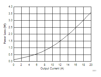
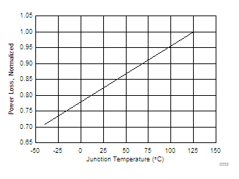
Test conditions: VIN = 12 V, VDD = 5 V, ƒSW = 500 kHz, VOUT = 1.3 V, LOUT = 0.95 µH, IOUT = 20 A, TJ = 125°C, unless stated otherwise.
CSD86336Q3D D001_SLPS666.gif
Figure 1. Power Loss vs Output Current
CSD86336Q3D D005_SLPS666.gif
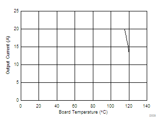
Figure 3. Typical Safe Operating Area (SOA) (1)
CSD86336Q3D D002_SLPS666.gif
Figure 2. Power Loss vs Temperature
CSD86336Q3D D006_SLPS666.gif
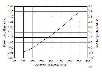
Figure 4. Normalized Power Loss vs Switching Frequency
CSD86336Q3D D008_SLPS666.gif
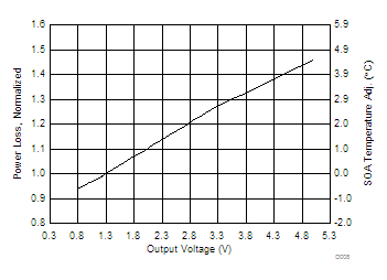
Figure 6. Normalized Power Loss vs Output Voltage
CSD86336Q3D D007_SLPS666.gif
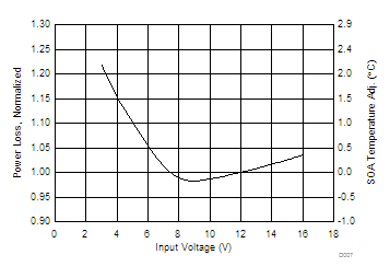
Figure 5. Normalized Power Loss vs Input Voltage
CSD86336Q3D D009_SLPS666.gif
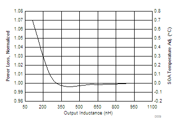
Figure 7. Normalized Power Loss vs Output Inductance
The Typical Power Block System Characteristic curves are based on measurements made on a PCB design with dimensions of 4 in (W) × 3.5 in (L) × 0.062 in (H) and 6 copper layers of 1-oz copper thickness. See Application and Implementation section for detailed explanation.