JAJSEY5 March 2018 CSD86336Q3D
PRODUCTION DATA.
- 1特長
- 2アプリケーション
- 3概要
- 4改訂履歴
-
5Specifications
- 5.1 Absolute Maximum Ratings
- 5.2 Recommended Operating Conditions
- 5.3 Thermal Information
- 5.4 Power Block Performance
- 5.5 Electrical Characteristics – Q1 Control FET
- 5.6 Electrical Characteristics – Q2 Sync FET
- 5.7 Typical Power Block Device Characteristics
- 5.8 Typical Power Block MOSFET Characteristics
- 6Application and Implementation
- 7Layout
- 8デバイスおよびドキュメントのサポート
- 9メカニカル、パッケージ、および注文情報
7.2.2 Thermal Performance
The power block has the ability to utilize the GND planes as the primary thermal path. As such, the use of thermal vias is an effective way to pull away heat from the device and into the system board. Concerns of solder voids and manufacturability problems can be addressed by the use of three basic tactics to minimize the amount of solder attach that will wick down the via barrel:
- Intentionally space out the vias from each other to avoid a cluster of holes in a given area.
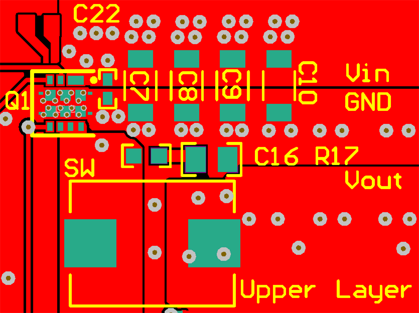
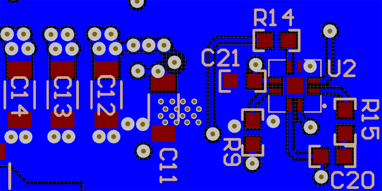
- Use the smallest drill size allowed in your design. The examples in Figure 33 and Figure 34 use vias with a 10-mil drill hole and a 16-mil capture pad.
- Tent the opposite side of the via with solder-mask.
In the end, the number and drill size of the thermal vias should align with the end user’s PCB design rules and manufacturing capabilities.
 Figure 33. Recommended PCB Layout (Top Down View)
 Figure 34. Recommended PCB Layout (Bottom View)