JAJSTV7 March 2024 DAC39RF10-SEP , DAC39RF10-SP , DAC39RFS10-SEP , DAC39RFS10-SP
PRODMIX
- 1
- 1 特長
- 2 アプリケーション
- 3 概要
- 4 Device Comparison
- 5 Pin Configuration and Functions
-
6 Specifications
- 6.1 Absolute Maximum Ratings
- 6.2 ESD Ratings
- 6.3 Recommended Operating Conditions
- 6.4 Thermal Information
- 6.5 Electrical Characteristics - DC Specifications
- 6.6 Electrical Characteristics - AC Specifications
- 6.7 Electrical Characteristics - Power Consumption
- 6.8 Timing Requirements
- 6.9 Switching Characteristics
- 6.10 SPI and FRI Timing Diagrams
- 6.11 Typical Characteristics: Bandwidth and DC Linearity
- 6.12 Typical Characteristics: Single Tone Spectra
- 6.13 Typical Characteristics: Dual Tone Spectra
- 6.14 Typical Characteristics: Noise Spectral Density
- 6.15 Typical Characteristics: Power Dissipation and Supply Currents
- 6.16 Typical Characteristics: Linearity Sweeps
- 6.17 Typical Characteristics: Modulated Waveforms
- 6.18 Typical Characteristics: Phase and Amplitude Noise
-
7 Detailed Description
- 7.1 Overview
- 7.2 Functional Block Diagrams
- 7.3
Feature Description
- 7.3.1 DAC Output Modes
- 7.3.2 DAC Core
- 7.3.3 DEM and Dither
- 7.3.4 Offset Adjustment
- 7.3.5 Clocking Subsystem
- 7.3.6 Digital Signal Processing Blocks
- 7.3.7
JESD204C Interface
- 7.3.7.1 Deviation from JESD204C Standard
- 7.3.7.2 Transport Layer
- 7.3.7.3 Scrambler and Descrambler
- 7.3.7.4 Link Layer
- 7.3.7.5 Physical Layer
- 7.3.7.6 Serdes PLL Control
- 7.3.7.7 Serdes Crossbar
- 7.3.7.8 Multi-Device Synchronization and Deterministic Latency
- 7.3.7.9 Operation in Subclass 0 Systems
- 7.3.7.10 Link Reset
- 7.3.8 Alarm Generation
- 7.4 Device Functional Modes
- 7.5 Programming
-
8 Application and Implementation
- 8.1 Application Information
- 8.2 Typical Application
- 8.3 Power Supply Recommendations
- 8.4 Layout
- 9 Device and Documentation Support
- 10Revision History
- 11Mechanical, Packaging, and Orderable Information
7.3.6 Digital Signal Processing Blocks
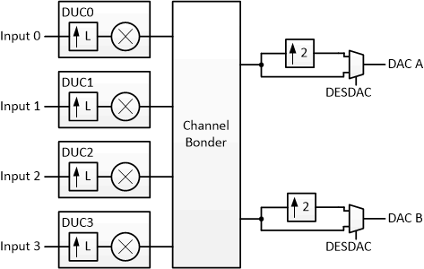
The digital signal processing blocks are shown in Figure 7-13. The device includes four digital up-converter (DUC) blocks supporting four complex (IQ) input streams that can be combined at different RF frequencies. The four DUCs can be flexibly assigned and summed together for either DAC output in the channel bonder. The final signal processing block is a extra interpolate by 2 filter for use with DES2XL/H mode.
Table 7-5 and Table 7-6 list the available modes for single channel and dual channel outputs, respectively.
 Figure 7-13 DUC Block with real output
| Input Steams | LT (Interpolation) | NCO_EN | DUC_FORMAT | DAC_SRC0 value | MXMODE0/1 | Description |
|---|---|---|---|---|---|---|
| 1 | 1 | 0 | Real | 0x1 | NRZ, RTZ, RF, DES2x | Single channel mode (no up-conversion). |
| 1 | 1 | 0 | Real | 0x1 | DES1x | Single channel mode with dual-edge samples w/o interpolation (DES1X). The JESD204C interface provides all samples (no interpolation). |
| 2, 4, 6 or 8 | 2-256x | 1 | Real | 0x1, 0x3, 0x7, 0xF | NRZ, RTZ, RF, DES2x | 1-4 DUC channels with single real output DAC_SRC0 settings are for 1, 2, 3, or 4 DUC channels respectively. |
| These modes only produce one output signal, so only one DAC is required. The table shows the programming to use DACA (MXMODE1 should be set to disabled). The user may elect to use DACB instead by programming DAC_SRC1 and MXMODE1 (and setting MXMODE0 to disabled). The user may also program DAC_SRC1=DAC_SRC0 and MXMODE1=MXMODE0 and then tie the DAC outputs together to get more output power. | ||||||
| Input Steams | LT (Interpolation) | NCO_EN | DUC_FORMAT | DAC_SRC0 value | DAC_SRC1 value | MXMODE0/1 | Description |
|---|---|---|---|---|---|---|---|
| 2 | 1 | 0 | N/A | 0x1 | 0x2 | NRZ, RTZ, RF, DES2x | Dual channel mode (no up-conversion) |
| 2, 4, 6 or 8 | 2-256x | 1 | Real | any bits set | any bits set | NRZ, RTZ, RF, DES2x | 1-4 DUC channels with two real outputs |
| 2 | 2-256x | 1 or 0 | Complex | 0x1 | 0x4 | NRZ, RTZ, RF, DES2x | 1 DUC channel with complex output: DACA outputs real samples DACB outputs imaginary samples |
| 4 | 2-256x | 1 or 0 | Complex | 0x3 | 0xC | NRZ, RTZ, RF, DES2x | 2 DUC channels with complex output |
| These modes produce two output signals (and uses both DACs). The user may elect to swap the values programmed into DAC_SRC0 and DAC_SRC1 to swap the output signals. Typically MXMODE0 and MXMODE1 are set to the same setting, however this is not required. | |||||||