JAJSML8 October 2020 DAC43401-Q1 , DAC53401-Q1
PRODUCTION DATA
- 1 特長
- 2 アプリケーション
- 3 概要
- 4 Revision History
- 5 Device Comparison Table
- 6 Pin Configuration and Functions
-
7 Specifications
- 7.1 Absolute Maximum Ratings
- 7.2 ESD Ratings
- 7.3 Recommended Operating Conditions
- 7.4 Thermal Information
- 7.5 Electrical Characteristics
- 7.6 Timing Requirements: I2C Standard Mode
- 7.7 Timing Requirements: I2C Fast Mode
- 7.8 Timing Requirements: I2C Fast Mode Plus
- 7.9 Typical Characteristics: VDD = 1.8 V (Reference = VDD) or VDD = 2 V (Internal Reference)
- 7.10 Typical Characteristics: VDD = 5.5 V (Reference = VDD) or VDD = 5 V (Internal Reference)
- 7.11 Typical Characteristics
-
8 Detailed Description
- 8.1 Overview
- 8.2 Functional Block Diagram
- 8.3 Feature Description
- 8.4 Device Functional Modes
- 8.5 Programming
- 8.6
Register Map
- 8.6.1 STATUS Register (address = D0h) [reset = 000Ch or 0014h]
- 8.6.2 GENERAL_CONFIG Register (address = D1h) [reset = 01F0h]
- 8.6.3 TRIGGER Register (address = D3h) [reset = 0008h]
- 8.6.4 DAC_DATA Register (address = 21h) [reset = 0000h]
- 8.6.5 DAC_MARGIN_HIGH Register (address = 25h) [reset = 0000h]
- 8.6.6 DAC_MARGIN_LOW Register (address = 26h) [reset = 0000h]
- 8.6.7 PMBUS_OPERATION Register (address = 01h) [reset = 0000h]
- 8.6.8 PMBUS_STATUS_BYTE Register (address = 78h) [reset = 0000h]
- 8.6.9 PMBUS_VERSION Register (address = 98h) [reset = 2200h]
- 9 Application and Implementation
- 10Power Supply Recommendations
- 11Layout
- 12Device and Documentation Support
- 13Mechanical, Packaging, and Orderable Information
パッケージ・オプション
メカニカル・データ(パッケージ|ピン)
- DSG|8
サーマルパッド・メカニカル・データ
- DSG|8
発注情報
8.3.8 PMBus Compatibility
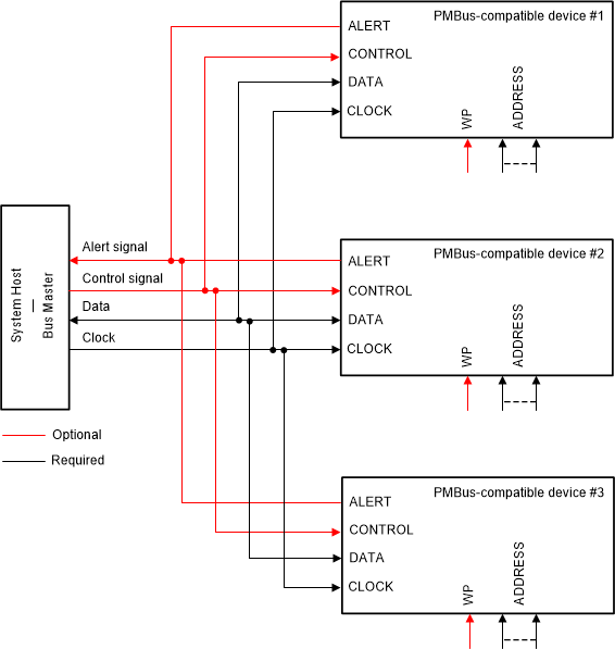
The PMBus protocol is an I2C-based communication standard for power-supply management. PMBus contains standard command codes tailored to power supply applications. The DACx3401-Q1 implement some PMBus commands such as Turn Off, Turn On, Margin Low, Margin High, Communication Failure Alert Bit (CML), as well as PMBUS revision. Figure 8-2 shows typical PMBus connections. The EN_PMBus bit (Bit 12, address D1h) must be set to 1 to enable the PMBus protocol.
 Figure 8-2 PMBus Connections
Similar to I2C, PMBus is a variable length packet of 8-bit data bytes, each with a receiver acknowledge, wrapped between a start and stop bit. The first byte is always a 7-bit slave address followed by a write bit, sometimes called the even address that identifies the intended receiver of the packet. The second byte is an 8-bit command byte, identifying the PMBus command being transmitted using the respective command code. After the command byte, the transmitter either sends data associated with the command to write to the receiver command register (from most significant byte to least significant byte), or sends a new start bit indicating the desire to read the data associated with the command register from the receiver. After, the receiver transmits the data following the same most significant byte first format (see Table 8-7).