JAJSML8 October 2020 DAC43401-Q1 , DAC53401-Q1
PRODUCTION DATA
- 1 特長
- 2 アプリケーション
- 3 概要
- 4 Revision History
- 5 Device Comparison Table
- 6 Pin Configuration and Functions
-
7 Specifications
- 7.1 Absolute Maximum Ratings
- 7.2 ESD Ratings
- 7.3 Recommended Operating Conditions
- 7.4 Thermal Information
- 7.5 Electrical Characteristics
- 7.6 Timing Requirements: I2C Standard Mode
- 7.7 Timing Requirements: I2C Fast Mode
- 7.8 Timing Requirements: I2C Fast Mode Plus
- 7.9 Typical Characteristics: VDD = 1.8 V (Reference = VDD) or VDD = 2 V (Internal Reference)
- 7.10 Typical Characteristics: VDD = 5.5 V (Reference = VDD) or VDD = 5 V (Internal Reference)
- 7.11 Typical Characteristics
-
8 Detailed Description
- 8.1 Overview
- 8.2 Functional Block Diagram
- 8.3 Feature Description
- 8.4 Device Functional Modes
- 8.5 Programming
- 8.6
Register Map
- 8.6.1 STATUS Register (address = D0h) [reset = 000Ch or 0014h]
- 8.6.2 GENERAL_CONFIG Register (address = D1h) [reset = 01F0h]
- 8.6.3 TRIGGER Register (address = D3h) [reset = 0008h]
- 8.6.4 DAC_DATA Register (address = 21h) [reset = 0000h]
- 8.6.5 DAC_MARGIN_HIGH Register (address = 25h) [reset = 0000h]
- 8.6.6 DAC_MARGIN_LOW Register (address = 26h) [reset = 0000h]
- 8.6.7 PMBUS_OPERATION Register (address = 01h) [reset = 0000h]
- 8.6.8 PMBUS_STATUS_BYTE Register (address = 78h) [reset = 0000h]
- 8.6.9 PMBUS_VERSION Register (address = 98h) [reset = 2200h]
- 9 Application and Implementation
- 10Power Supply Recommendations
- 11Layout
- 12Device and Documentation Support
- 13Mechanical, Packaging, and Orderable Information
パッケージ・オプション
メカニカル・データ(パッケージ|ピン)
- DSG|8
サーマルパッド・メカニカル・データ
- DSG|8
発注情報
8.5.2 I2C Update Sequence
| MSB | .... | LSB | ACK | MSB | ... | LSB | ACK | MSB | ... | LSB | ACK | MSB | ... | LSB | ACK |
|---|---|---|---|---|---|---|---|---|---|---|---|---|---|---|---|
| Address (A) byte Section 8.5.2.1 |
Command byte Section 8.5.2.2 |
Data byte - MSDB | Data byte - LSDB | ||||||||||||
| DB [31:24] | DB [23:16] | DB [15:8] | DB [7:0] | ||||||||||||
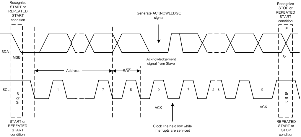
After each byte is received, the DACx3401-Q1 family acknowledges the byte by pulling the SDA line low during the high period of a single clock pulse, as shown in Figure 8-6. These four bytes and acknowledge cycles make up the 36 clock cycles required for a single update to occur. A valid I2C address byte selects the DACx3401-Q1 devices.
 Figure 8-6 I2C Bus
Protocol
Figure 8-6 I2C Bus
ProtocolThe command byte sets the operating mode of the selected DACx3401-Q1 device. For a data update to occur when the operating mode is selected by this byte, the DACx3401-Q1 device must receive two data bytes: the most significant data byte (MSDB) and least significant data byte (LSDB). The DACx3401-Q1 device performs an update on the falling edge of the acknowledge signal that follows the LSDB.
When using fast mode (clock = 400 kHz), the maximum DAC update rate is limited to 10 kSPS. Using the fast mode plus (clock = 1 MHz), the maximum DAC update rate is limited to 25 kSPS. When a stop condition is received, the DACx3401-Q1 device releases the I2C bus and awaits a new start condition.