JAJSJY6 december 2020 DAC43701 , DAC53701
PRODUCTION DATA
- 1
- 1 特長
- 2 アプリケーション
- 3 概要
- 4 Revision History
- 5 Device Comparison Table
- 6 Pin Configuration and Functions
-
7 Specifications
- 7.1 Absolute Maximum Ratings
- 7.2 ESD Ratings
- 7.3 Recommended Operating Conditions
- 7.4 Thermal Information
- 7.5 Electrical Characteristics
- 7.6 Timing Requirements: I2C Standard Mode
- 7.7 Timing Requirements: I2C Fast Mode
- 7.8 Timing Requirements: I2C Fast Mode Plus
- 7.9 Timing Requirements: GPI
- 7.10 Timing Diagram
- 7.11 Typical Characteristics: VDD = 5.5 V (Reference = VDD) or VDD = 5 V (Internal Reference)
- 7.12 Typical Characteristics: VDD = 1.8 V (Reference = VDD) or VDD = 2 V (Internal Reference)
- 7.13 Typical Characteristics
-
8 Detailed Description
- 8.1 Overview
- 8.2 Functional Block Diagram
- 8.3 Feature Description
- 8.4 Device Functional Modes
- 8.5 Programming
- 8.6
Register Map
- 8.6.1 STATUS Register (address = D0h) [reset = 000Ch or 0014h]
- 8.6.2 GENERAL_CONFIG Register (address = D1h) [reset = 01F0h]
- 8.6.3 CONFIG2 Register (address = D2h) [reset = 0000h]
- 8.6.4 TRIGGER Register (address = D3h) [reset = 0008h]
- 8.6.5 DAC_DATA Register (address = 21h) [reset = 0000h]
- 8.6.6 DAC_MARGIN_HIGH Register (address = 25h) [reset = 0000h]
- 8.6.7 DAC_MARGIN_LOW Register (address = 26h) [reset = 0000h]
- 8.6.8 PMBUS_OPERATION Register (address = 01h) [reset = 0000h]
- 8.6.9 PMBUS_STATUS_BYTE Register (address = 78h) [reset = 0000h]
- 8.6.10 PMBUS_VERSION Register (address = 98h) [reset = 2200h]
- 9 Application and Implementation
- 10Power Supply Recommendations
- 11Layout
- 12Device and Documentation Support
- 13Mechanical, Packaging, and Orderable Information
8.5 Programming
The DACx3701 devices have a 2-wire serial interface (SCL and SDA) as shown in the pin diagram of Section 6. The I2C bus consists of a data line (SDA) and a clock line (SCL) with pullup structures. When the bus is idle, both SDA and SCL lines are pulled high. All the I2C-compatible devices connect to the I2C bus through the open drain I/O pins, SDA and SCL.
The I2C specification states that the device that controls communication is called a master, and the devices that are controlled by the master are called slaves. The master device generates the SCL signal. The master device also generates special timing conditions (start condition, repeated start condition, and stop condition) on the bus to indicate the start or stop of a data transfer. Device addressing is completed by the master. The master device on an I2C bus is typically a microcontroller or digital signal processor (DSP). The DACx3701 family operates as a slave device on the I2C bus. A slave device acknowledges master commands, and upon master control, receives or transmits data.
Typically, theDACx3701 family operates as a slave receiver. A master device writes to the DACx3701, a slave receiver. However, if a master device requires the DACx3701 internal register data, the DACx3701 operate as a slave transmitter. In this case, the master device reads from the DACx3701. According to I2C terminology, read and write refer to the master device.
The DACx3701 family is a slave and supports the following data transfer modes:
- Standard mode (100 kbps)
- Fast mode (400 kbps)
- Fast mode plus (1.0 Mbps)
The data transfer protocol for standard and fast modes is exactly the same; therefore, both modes are referred to as F/S-mode in this document. The fast mode plus protocol is supported in terms of data transfer speed, but not output current. The low-level output current would be 3 mA; similar to the case of standard and fast modes. The DACx3701 family supports 7-bit addressing. The 10-bit addressing mode is not supported. The device supports the general call reset function. Sending the following sequence initiates a software reset within the device: start or repeated start, 0x00, 0x06, stop. The reset is asserted within the device on the rising edge of the ACK bit, following the second byte.
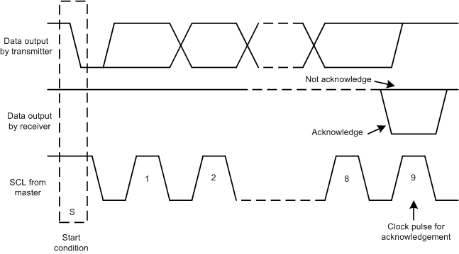
Other than specific timing signals, the I2C interface works with serial bytes. At the end of each byte, a ninth clock cycle generates and detects an acknowledge signal. An acknowledge is when the SDA line is pulled low during the high period of the ninth clock cycle. A not-acknowledge is when the SDA line is left high during the high period of the ninth clock cycle, as shown in Figure 8-3.
 Figure 8-3 Acknowledge and Not Acknowledge on the
I2C Bus