JAJSE78C August 2017 – January 2019 DAC60504 , DAC70504 , DAC80504
PRODUCTION DATA.
- 1 特長
- 2 アプリケーション
- 3 概要
- 4 改訂履歴
- 5 概要(続き)
- 6 Device Comparison Table
- 7 Pin Configuration and Functions
- 8 Specifications
-
9 Detailed Description
- 9.1 Overview
- 9.2 Functional Block Diagram
- 9.3 Feature Description
- 9.4 Device Functional Modes
- 9.5 Programming
- 9.6
Register Map
- 9.6.1 NOP Register (address = 0x00) [reset = 0x0000]
- 9.6.2 DEVICE ID Register (address = 0x01) [reset = 0x---]
- 9.6.3 SYNC Register (address = 0x2) [reset = 0xFF00]
- 9.6.4 CONFIG Register (address = 0x3) [reset = 0x0000]
- 9.6.5 GAIN Register (address = 0x04) [reset = 0x---]
- 9.6.6 TRIGGER Register (address = 0x05) [reset = 0x0000]
- 9.6.7 BRDCAST Register (address = 0x6) [reset = 0x0000]
- 9.6.8 STATUS Register (address = 0x7) [reset = 0x0000]
- 9.6.9 DACx Register (address = 0x8 to 0xF) [reset = 0x0000 or 0x8000]
- 10Application and Implementation
- 11Power Supply Recommendations
- 12Layout
- 13デバイスおよびドキュメントのサポート
- 14メカニカル、パッケージ、および注文情報
パッケージ・オプション
メカニカル・データ(パッケージ|ピン)
- RTE|16
サーマルパッド・メカニカル・データ
- RTE|16
発注情報
9.3.3.1 Power-on-Reset (POR)
The DACx0504 includes a power-on reset function that controls the output voltage at power up. After the VDD and VIO supplies have been established a POR event is issued. The POR causes all registers to initialize to their default values and communication with the device is valid only after a 250 µs power-on-reset delay. The default value for all DACs is either zero-code or midscale-code as determined by the RSTSEL pin. Each DAC channel remains at the power-up voltage until a valid command is written to it.
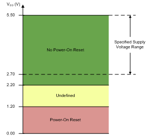
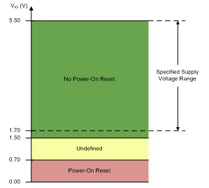
The POR circuit requires specific supply levels to discharge the internal capacitors and to reset the device on power up, as indicated in Figure 59 and Figure 60. In order to initiate a POR event, VDD or VIO must be below their corresponding low thresholds for at least 100 µs. If VDD and VIO remain above their specified high threshold a POR event will not occur. When the supplies drop below their high threshold but remain over the lower one (shown as the undefined region), the device may or may not reset under all specified temperature and power-supply conditions.
 Figure 59. Threshold Levels for VDD POR Circuit
  Figure 60. Threshold Levels for VIO POR Circuit