JAJSE78C August   2017  – January 2019 DAC60504 , DAC70504 , DAC80504

PRODUCTION DATA.  

  1. 特長
  2. アプリケーション
  3. 概要
    1.     Device Images
      1.      ブロック概略図
  4. 改訂履歴
  5. 概要(続き)
  6. Device Comparison Table
  7. Pin Configuration and Functions
    1.     Pin Functions
  8. Specifications
    1. 8.1 Absolute Maximum Ratings
    2. 8.2 ESD Ratings
    3. 8.3 Recommended Operating Conditions
    4. 8.4 Thermal Information
    5. 8.5 Electrical Characteristics
    6. 8.6 Typical Characteristics
  9. Detailed Description
    1. 9.1 Overview
    2. 9.2 Functional Block Diagram
    3. 9.3 Feature Description
      1. 9.3.1 Digital-to-Analog Converter (DAC)
        1. 9.3.1.1 DAC Transfer Function
        2. 9.3.1.2 Output Amplifiers
        3. 9.3.1.3 DAC Register Structure
          1. 9.3.1.3.1 DAC Register Synchronous and Asynchronous Updates
          2. 9.3.1.3.2 Broadcast DAC Register
      2. 9.3.2 Internal Reference
        1. 9.3.2.1 Reference Divider
        2. 9.3.2.2 Solder Heat Reflow
      3. 9.3.3 Device Reset Options
        1. 9.3.3.1 Power-on-Reset (POR)
        2. 9.3.3.2 Software Reset
    4. 9.4 Device Functional Modes
      1. 9.4.1 Stand-Alone Operation
      2. 9.4.2 Daisy-Chain Operation
      3. 9.4.3 Frame Error Checking
      4. 9.4.4 Power-Down Mode
    5. 9.5 Programming
    6. 9.6 Register Map
      1. 9.6.1 NOP Register (address = 0x00) [reset = 0x0000]
        1. Table 9. NOP Register Field Descriptions
      2. 9.6.2 DEVICE ID Register (address = 0x01) [reset = 0x---]
        1. Table 10. DEVICE ID Field Descriptions
      3. 9.6.3 SYNC Register (address = 0x2) [reset = 0xFF00]
        1. Table 11. SYNC Register Field Descriptions
      4. 9.6.4 CONFIG Register (address = 0x3) [reset = 0x0000]
        1. Table 12. CONFIG Register Field Descriptions
      5. 9.6.5 GAIN Register (address = 0x04) [reset = 0x---]
        1. Table 13. GAIN Register Field Descriptions
      6. 9.6.6 TRIGGER Register (address = 0x05) [reset = 0x0000]
        1. Table 14. TRIGGER Register Field Descriptions
      7. 9.6.7 BRDCAST Register (address = 0x6) [reset = 0x0000]
        1. Table 15. BRDCAST Register Field Descriptions
      8. 9.6.8 STATUS Register (address = 0x7) [reset = 0x0000]
        1. Table 16. STATUS Register Field Descriptions
      9. 9.6.9 DACx Register (address = 0x8 to 0xF) [reset = 0x0000 or 0x8000]
        1. Table 17. DACx Register Field Descriptions
  10. 10Application and Implementation
    1. 10.1 Application Information
      1. 10.1.1 Interfacing to a Microcontroller
      2. 10.1.2 Programmable Current Source Circuit
    2. 10.2 Typical Application
      1. 10.2.1 Design Requirements
      2. 10.2.2 Detailed Design Procedure
      3. 10.2.3 Application Curve
  11. 11Power Supply Recommendations
  12. 12Layout
    1. 12.1 Layout Guidelines
    2. 12.2 Layout Example
  13. 13デバイスおよびドキュメントのサポート
    1. 13.1 ドキュメントのサポート
      1. 13.1.1 関連資料
    2. 13.2 関連リンク
    3. 13.3 ドキュメントの更新通知を受け取る方法
    4. 13.4 コミュニティ・リソース
    5. 13.5 商標
    6. 13.6 静電気放電に関する注意事項
    7. 13.7 Glossary
  14. 14メカニカル、パッケージ、および注文情報

パッケージ・オプション

メカニカル・データ(パッケージ|ピン)
サーマルパッド・メカニカル・データ
発注情報

Typical Characteristics

at TA = 25°C, VDD = 5.5 V, internal reference = 2.5 V, gain = 2, DAC outputs unloaded (unless otherwise noted)
DAC80504 DAC70504 DAC60504 D001.gif
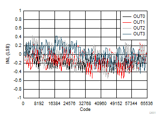
Figure 1. Integral Linearity Error vs Digital Input Code
DAC80504 DAC70504 DAC60504 D003.gif
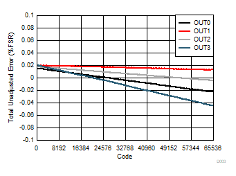
Figure 3. Total Unadjusted Error vs Digital Input Code
DAC80504 DAC70504 DAC60504 D005.gif
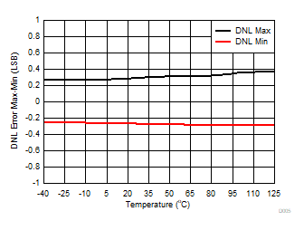
Figure 5. Differential Linearity Error vs Temperature
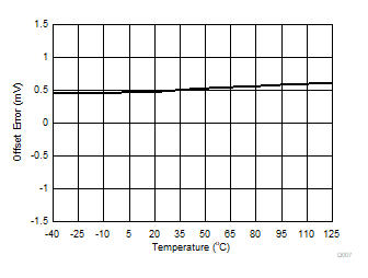
DAC80504 DAC70504 DAC60504 D007.gif
Figure 7. Offset Error vs Temperature
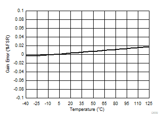
DAC80504 DAC70504 DAC60504 D009.gif
Figure 9. Gain Error vs Temperature
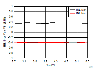
DAC80504 DAC70504 DAC60504 D011.gif
Gain = 1
Figure 11. Integral Linearity Error vs Supply Voltage
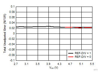
DAC80504 DAC70504 DAC60504 D013.gif
Gain = 1
Figure 13. Total Unadjusted Error vs Supply Voltage
DAC80504 DAC70504 DAC60504 D015.gif
Gain = 1
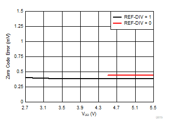
Figure 15. Zero Code Error vs Supply Voltage
DAC80504 DAC70504 DAC60504 D017.gif
Gain = 1
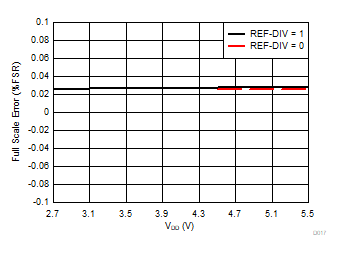
Figure 17. Full Scale Error vs Supply Voltage
DAC80504 DAC70504 DAC60504 D019_SLASEL1.gif
Gain = 1
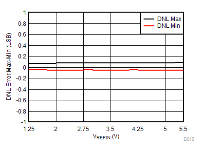
Figure 19. Differential Linearity Error vs Reference Voltage
DAC80504 DAC70504 DAC60504 D021.gif
Gain = 1
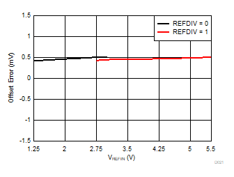
Figure 21. Offset Error vs Reference Voltage
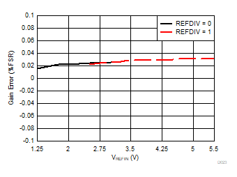
DAC80504 DAC70504 DAC60504 D023.gif
Gain = 1
Figure 23. Gain Error vs Reference Voltage
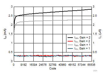
DAC80504 DAC70504 DAC60504 D025.gif
Gain = 1, external reference = 2.5 V
Figure 25. Supply Current With External Reference vs
Digital Input Code
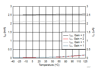
DAC80504 DAC70504 DAC60504 D027.gif
Gain = 1, external reference = 2.5 V
Figure 27. Supply Current With External Reference vs
Temperature
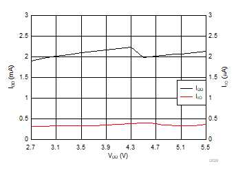
DAC80504 DAC70504 DAC60504 D029.gif
Gain = 1, external reference = 2.5 V
Figure 29. Supply Current With External Reference vs
Supply Voltage
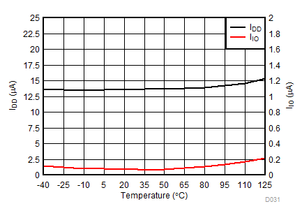
DAC80504 DAC70504 DAC60504 D031.gif
Figure 31. Supply Current and Input Current vs Temperature
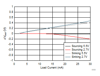
DAC80504 DAC70504 DAC60504 D033.gif
Figure 33. Headroom/Footroom vs Load Current
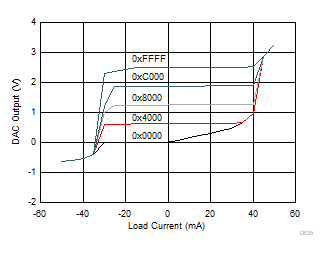
DAC80504 DAC70504 DAC60504 D035.gif
Figure 35. Source and Sink Capability With Gain = 1
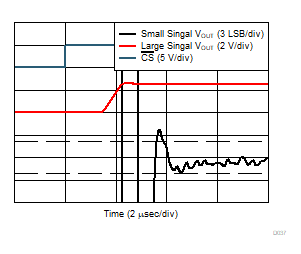
DAC80504 DAC70504 DAC60504 D037.gif
Gain = 1
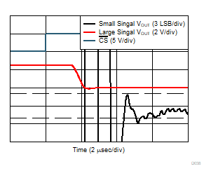
Figure 37. Full-Scale Settling Time, Rising Edge
DAC80504 DAC70504 DAC60504 D039.gif
Gain = 1
Figure 39. Glitch Impulse, Falling Edge, 1 LSB Step
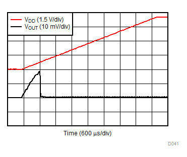
DAC80504 DAC70504 DAC60504 D041.gif
Gain = 1
Figure 41. Power-On, Reset to Zero Scale
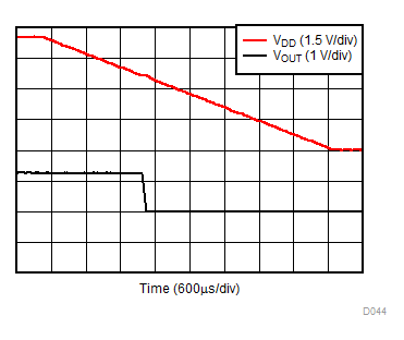
DAC80504 DAC70504 DAC60504 D044.gif
Gain = 1, DAC code at midscale
Figure 43. VDD Power-Down
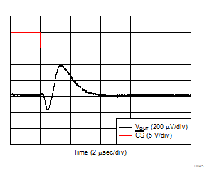
DAC80504 DAC70504 DAC60504 D045.gif
Gain = 1, measured DAC at midscale,
all other DACs switch from code 32 to full scale
Figure 45. Channel to Channel Crosstalk
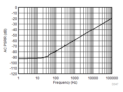
DAC80504 DAC70504 DAC60504 D047.gif
Gain = 1, VDD = 5 V + 200 mVPP (Sinusoid), DAC code at fullscale
Figure 47. DAC Output AC PSRR vs Frequency
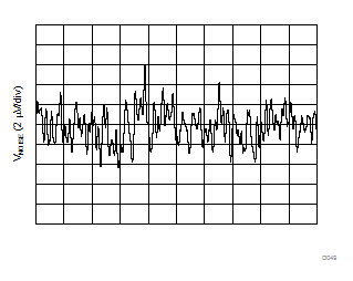
DAC80504 DAC70504 DAC60504 D049.gif
Gain = 1, external reference = 2.5 V, DAC code at midscale
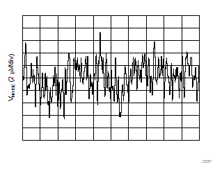
Figure 49. DAC Output Noise With External Reference
0.1 Hz to 10 Hz
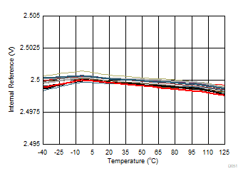
DAC80504 DAC70504 DAC60504 D051.gif
Figure 51. Internal Reference Voltage vs Temperature
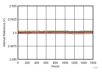
DAC80504 DAC70504 DAC60504 D055.gif
Figure 53. Internal Reference Voltage vs Time
DAC80504 DAC70504 DAC60504 D057.gif
0.1 Hz to 10 Hz
Figure 55. Internal Reference Noise
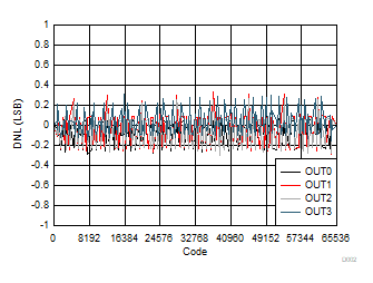
DAC80504 DAC70504 DAC60504 D002.gif
Figure 2. Differential Linearity Error vs Digital Input Code
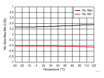
DAC80504 DAC70504 DAC60504 D004.gif
Figure 4. Integral Linearity Error vs Temperature
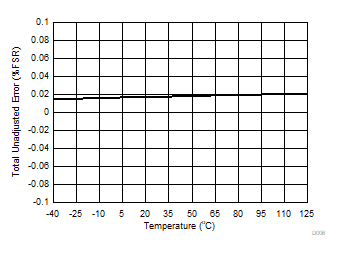
DAC80504 DAC70504 DAC60504 D006.gif
Figure 6. Total Unadjusted Error vs Temperature
DAC80504 DAC70504 DAC60504 D008.gif
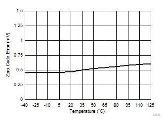
Figure 8. Zero Code Error vs Temperature
DAC80504 DAC70504 DAC60504 D010.gif
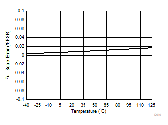
Figure 10. Full Scale Error vs Temperature
DAC80504 DAC70504 DAC60504 D012.gif
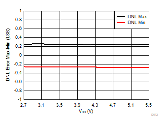
Gain = 1
Figure 12. Differential Linearity Error vs Supply Voltage
DAC80504 DAC70504 DAC60504 D014.gif
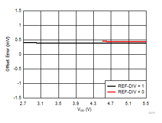
Gain = 1
Figure 14. Offset Error vs Supply Voltage
DAC80504 DAC70504 DAC60504 D016.gif
Gain = 1
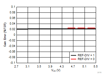
Figure 16. Gain Error vs Supply Voltage
DAC80504 DAC70504 DAC60504 D018.gif
Gain = 1
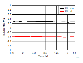
Figure 18. Integral Linearity Error vs Reference Voltage
DAC80504 DAC70504 DAC60504 D020.gif
Gain = 1
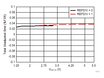
Figure 20. Total Unadjusted Error vs Reference Voltage
DAC80504 DAC70504 DAC60504 D022.gif
Gain = 1
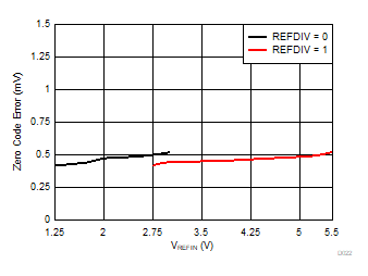
Figure 22. Zero Code Error vs Reference Voltage
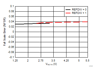
DAC80504 DAC70504 DAC60504 D024.gif
Gain = 1
Figure 24. Full Scale Error vs Reference Voltage
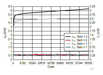
DAC80504 DAC70504 DAC60504 D026.gif
Gain = 1
Figure 26. Supply Current With Internal Reference vs
Digital Input Code
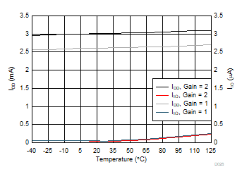
DAC80504 DAC70504 DAC60504 D028.gif
Gain = 1
Figure 28. Supply Current With Internal Reference vs
Temperature
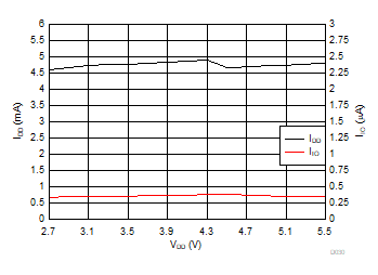
DAC80504 DAC70504 DAC60504 D030.gif
Gain = 1
Figure 30. Supply Current With Internal Reference vs
Supply Voltage
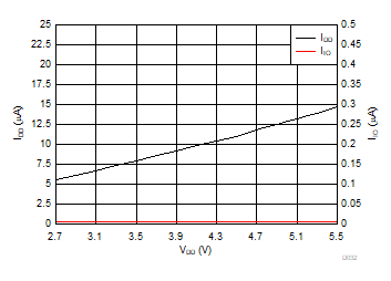
DAC80504 DAC70504 DAC60504 D032.gif
Figure 32. Supply Current and Input Current vs Supply Voltage
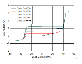
DAC80504 DAC70504 DAC60504 D034.gif
Figure 34. Source and Sink Capability With Gain = ½
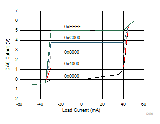
DAC80504 DAC70504 DAC60504 D036.gif
Figure 36. Source and Sink Capability With Gain = 2
DAC80504 DAC70504 DAC60504 D038.gif
Gain = 1
Figure 38. Full-Scale Settling Time, Falling Edge
DAC80504 DAC70504 DAC60504 D040.gif
Gain = 1
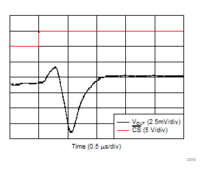
Figure 40. Glitch Impulse, Rising Edge, 1 LSB Step
DAC80504 DAC70504 DAC60504 D042.gif
Gain = 1
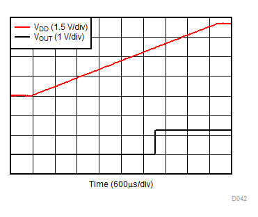
Figure 42. Power-On, Reset to Midscale
DAC80504 DAC70504 DAC60504 D060_SLASEL1.gif
Gain = 1, DAC code at midscale
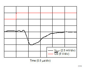
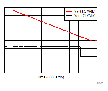
Figure 44. VIO Power-Down
DAC80504 DAC70504 DAC60504 D046.gif
Gain = 1, DAC code at midscale
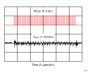
Figure 46. Clock Feedthrough With SCLK = 1 MHz
DAC80504 DAC70504 DAC60504 D048.gif
External reference = 2.5 V, DAC code at midscale
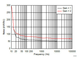
Figure 48. DAC Output Noise Density vs Frequency
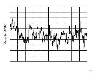
DAC80504 DAC70504 DAC60504 D050.gif
Gain = 1, DAC code at midscale
Figure 50. DAC Output Noise With Internal Reference
0.1 Hz to 10 Hz
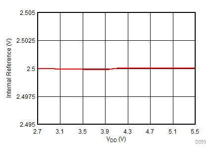
DAC80504 DAC70504 DAC60504 D053.gif
Figure 52. Internal Reference Voltage vs Supply Voltage
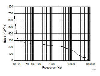
DAC80504 DAC70504 DAC60504 D056_SLASEL1.gif
Figure 54. Internal Reference Noise Density vs Frequency
DAC80504 DAC70504 DAC60504 D058.gif
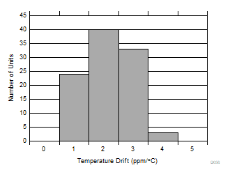
Figure 56. Internal Reference Temperature Drift Histogram