SLAS767B June 2011 – March 2015 DAC7551-Q1
PRODUCTION DATA.
- 1 Features
- 2 Applications
- 3 Description
- 4 Revision History
- 5 Pin Configuration and Functions
- 6 Specifications
- 7 Detailed Description
- 8 Application and Implementation
- 9 Power Supply Recommendations
- 10Layout
- 11Device and Documentation Support
- 12Mechanical, Packaging, and Orderable Information
8 Application and Implementation
NOTE
Information in the following applications sections is not part of the TI component specification, and TI does not warrant its accuracy or completeness. TI’s customers are responsible for determining suitability of components for their purposes. Customers should validate and test their design implementation to confirm system functionality.
8.1 Application Information
8.1.1 Waveform Generation
As a result of the exceptional linearity and low glitch of the DAC7551-Q1 device, the device is well-suited for waveform generation (from DC to 10kHz). The DAC7551-Q1 large-signal settling time is 5 μs, supporting an update rate of 200 kSPS. However, the update rates can exceed 1 MSPS if the waveform to be generated consists of small voltage steps between consecutive DAC updates. To obtain a high dynamic range, the REF3140 device (4.096 V) or the REF02 device (5 V) is recommended for reference-voltage generation.
8.1.2 Generating ±5-V, ±10-V, and ±12-V Outputs For Precision Industrial Control
Industrial control applications can require multiple feedback loops consisting of sensors, analog-to-digital converters (ADCs), microcontrollers (MCUs), DACs, and actuators. Loop accuracy and loop speed are the two important parameters of such control loops.
8.1.2.1 Loop Accuracy
DAC offset, gain, and the integral linearity errors are not factors in determining the accuracy of the loop. As long as a voltage exists in the transfer curve of a monotonic DAC, the loop can find this voltage and settle to it. On the other hand, DAC resolution and differential linearity do determine the loop accuracy, because each DAC step determines the minimum incremental change the loop can generate. A DNL error less than –1 LSB (non-monotonicity) can create loop instability. A DNL error greater than 1 LSB implies unnecessarily large voltage steps and missed voltage targets. With high DNL errors, the loop loses stability, resolution, and accuracy. Offering 12-bit ensured monotonicity and ±0.08-LSB typical DNL error, the DAC755x devices are great choices for precision control loops.
8.1.2.2 Loop Speed
Many factors determine the control-loop speed, such as ADC conversion time, MCU speed, and DAC settling time. Typically, the ADC conversion time, and the MCU computation time are the two major factors that dominate the time constant of the loop. DAC settling time is rarely a dominant factor because ADC conversion times usually exceed DAC conversion times. DAC offset, gain, and linearity errors can slow the loop down only during the startup. When the loop reaches the steady-state operation, these errors do not affect loop speed any further. Depending on the ringing characteristics of the loop-transfer function, DAC glitches can also slow the loop down. With a 1-MSPS (small-signal) maximum data-update rate, the DAC7551-Q1 device can support high-speed control loops. Ultralow glitch energy of the DAC7551-Q1 device significantly improves loop stability and loop settling time.
8.2 Typical Application
8.2.1 Generating Industrial Voltage Ranges
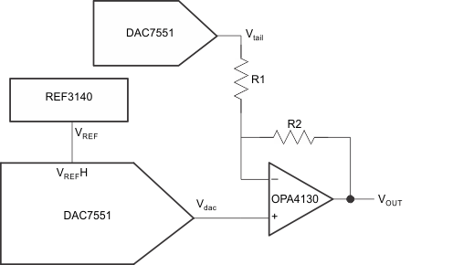
For control-loop applications, DAC gain and offset errors are not important parameters. This consideration could be exploited to lower trim and calibration costs in a high-voltage control-circuit design. Using a quad operational amplifier (OPA4130), and a voltage reference (REF3140), the DAC7551-Q1 can generate the wide voltage swings required by the control loop.
 Figure 28. Low-cost, Wide-swing Voltage Generator for Control-Loop Applications
8.2.1.1 Design Requirements
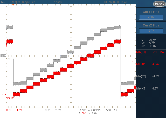
For ±5-V operation:
R1 = 10 kΩ
R2 = 15 kΩ
Vtail = 3.33 V
VREF = 4.096 V
For ±10-V operation:
R1 = 10 kΩ
R2 = 39 kΩ
Vtail = 2.56 V
VREF = 4.096 V
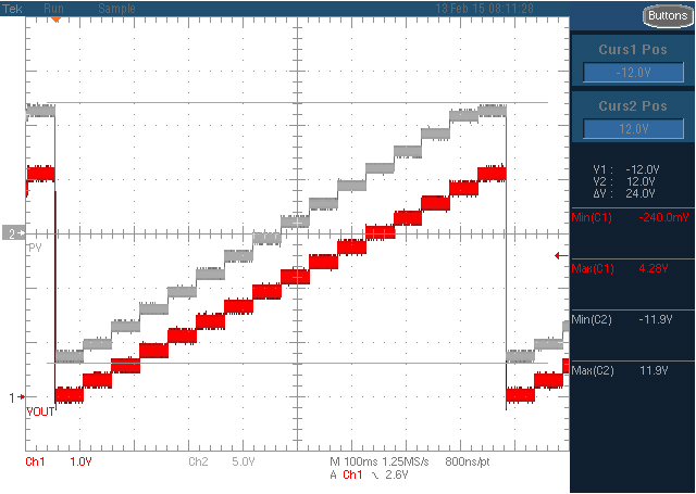
For ±12-V operation:
R1 = 10 kΩ
R2 = 49 kΩ
Vtail = 2.45 V
VREF = 4.096 V
8.2.1.2 Detailed Design Procedure
Use Equation 2 to calculate the output voltage of the configuration.

Fixed R1 and R2 resistors can be used to coarsely set the gain required in the first term of the equation. When R2 and R1 set the gain to include some minimal over-range gain, a single DAC7551-Q1 device can be used to set the required offset voltages. Residual errors are not an issue for loop accuracy because offset and gain errors can be tolerated. One DAC7551-Q1 device can provide the Vtail voltages, while four additional DAC7551-Q1 devices can provide the Vdac voltages to generate four high-voltage outputs. A single SPI is sufficient to control all five DAC7551-Q1 devices in a daisy-chain configuration.
8.2.1.3 Application Curves

±5-V Operation

±12-V Operation

±10-V Operation