SLAS767B June 2011 – March 2015 DAC7551-Q1
PRODUCTION DATA.
- 1 Features
- 2 Applications
- 3 Description
- 4 Revision History
- 5 Pin Configuration and Functions
- 6 Specifications
- 7 Detailed Description
- 8 Application and Implementation
- 9 Power Supply Recommendations
- 10Layout
- 11Device and Documentation Support
- 12Mechanical, Packaging, and Orderable Information
6 Specifications
6.1 Absolute Maximum Ratings
Over operating free-air temperature range (unless otherwise noted).(1)| MIN | MAX | UNIT | |
|---|---|---|---|
| VDD , IOVDD to GND | –0.3 | 6 | V |
| Digital input voltage to GND | –0.3 | VDD + 0.3 | V |
| VOUT to GND | –0.3 | VDD + 0.3 | V |
| Operating temperature range | –40 | 105 | °C |
| Junction temperature, TJ max | 150 | °C | |
| Power dissipation (DRN) | (TJ max – TA) / RθJA | ||
| Storage temperature, Tstg | –65 | 150 | °C |
(1) Stresses above those listed under Absolute Maximum Ratings may cause permanent damage to the device. Exposure to absolute maximum conditions for extended periods may affect device reliability.
6.2 ESD Ratings
| VALUE | UNIT | ||||
|---|---|---|---|---|---|
| V(ESD) | Electrostatic discharge | Human-body model (HBM), per AEC Q100-002(1) | ±2000 | V | |
| Charged-device model (CDM), per AEC Q100-011 | All pins | ±500 | |||
| Corner pins (1, 6, 7, and 12) | ±750 | ||||
(1) AEC Q100-002 indicates that HBM stressing shall be in accordance with the ANSI/ESDA/JEDEC JS-001 specification.
6.3 Recommended Operating Conditions
over operating free-air temperature range (unless otherwise noted)| MIN | NOM | MAX | UNIT | |||
|---|---|---|---|---|---|---|
| VI | Input voltage | VDD | 2.7 | 5.5 | V | |
| VREFH | 0.25 | VDD | ||||
| VREFL | 0 | GND | VDD | |||
| VFB | 0 | VDD | ||||
| IOVDD | 1.8 | VDD | ||||
| CLR | 0 | IOVDD | ||||
| SYNC | 0 | IOVDD | ||||
| SCLK | 0 | IOVDD | ||||
| SDIN | 0 | IOVDD | ||||
| VO | Output voltage | SDO | 0 | IOVDD | V | |
| VOUT | 0 | VDD | ||||
| TJ | Operating junction temperature | 150 | °C | |||
6.4 Thermal Information
| THERMAL METRIC(1) | DRN (USON) | UNIT | |
|---|---|---|---|
| 12 PINS | |||
| RθJA | Junction-to-ambient thermal resistance | 49.8 | °C/W |
| RθJC(top) | Junction-to-case (top) thermal resistance | 45.8 | |
| RθJB | Junction-to-board thermal resistance | 18.2 | |
| ψJT | Junction-to-top characterization parameter | 0.8 | |
| ψJB | Junction-to-board characterization parameter | 18.3 | |
| RθJC(bot) | Junction-to-case (bottom) thermal resistance | 2.9 | |
(1) For more information about traditional and new thermal metrics, see the IC Package Thermal Metrics application report, SPRA953.
6.5 Electrical Characteristics
all specifications at –40°C to +105°C, VDD = 2.7 to 5.5 V, VREFH = VDD, VREFL = GND, RL = 2 kΩ to GND, and CL = 200 pF to GND (unless otherwise noted).| PARAMETER | TEST CONDITIONS | MIN | TYP | MAX | UNIT | ||
|---|---|---|---|---|---|---|---|
| STATIC PERFORMANCE(1) | |||||||
| Resolution | 12 | Bits | |||||
| Relative accuracy | ±0.35 | ±1 | LSB | ||||
| Differential nonlinearity | Specified monotonic by design | ±0.08 | ±0.5 | LSB | |||
| Offset error | ±12 | mV | |||||
| Zero-scale error | All zeroes loaded to DAC register | ±12 | mV | ||||
| Gain error | ±0.15 | %FSR | |||||
| Full-scale error | ±0.5 | %FSR | |||||
| Zero-scale error drift | 7 | μV/°C | |||||
| Gain temperature coefficient | 3 | ppm of FSR/°C | |||||
| PSRR | Power-supply rejection ratio | VDD = 5 V | 0.75 | mV/V | |||
| OUTPUT CHARACTERISTICS(2) | |||||||
| Output voltage range | 2 × VREFL | VREFH | V | ||||
| Output voltage settling time | RL = 2 kΩ, 0 pF < CL < 200 pF | 5 | μs | ||||
| Slew rate | 1.8 | V/μs | |||||
| Capacitive load stability | RL = ∞ | 470 | pF | ||||
| RL = 2 kΩ | 1000 | ||||||
| Digital-to-analog glitch impulse | 1 LSB change around major carry | 0.1 | nV-s | ||||
| Digital feedthrough | 0.1 | nV-s | |||||
| Output noise density | 10kHz offset frequency | 120 | nV/√Hz | ||||
| THD | Total harmonic distortion | fOUT = 1 kHz, fS = 1 MSPS, BW = 20 kHz | –85 | dB | |||
| DC output impedance | 1 | Ω | |||||
| Short-circuit current | VDD = 5 V | 50 | mA | ||||
| VDD = 3 V | 20 | ||||||
| Power-up time | Coming out of power-down mode, VDD = 5 V | 15 | μs | ||||
| Coming out of power-down mode, VDD = 3 V | 15 | ||||||
| REFERENCE INPUT | |||||||
| VREFH input range | 0 | VDD | V | ||||
| VREFL input range | VREFL < VREFH | 0 | GND | VDD | V | ||
| Reference input impedance | 100 | kΩ | |||||
| Reference current | VREF = VDD = 5 V | 50 | 100 | μA | |||
| VREF = VDD = 3 V | 30 | 60 | |||||
| LOGIC INPUTS(2) | |||||||
| Input current | ±1 | μA | |||||
| VIN_L | Input low voltage | IOVDD ≥ 2.7 V | 0.3 IOVDD | V | |||
| VIN_H | Input high voltage | IOVDD ≥ 2.7 V | 0.7 IOVDD | V | |||
| Pin capacitance | 3 | pF | |||||
| POWER REQUIREMENTS | |||||||
| VDD | Supply voltage | 2.7 | 5.5 | V | |||
| IOVDD | I/O supply voltage(3) | 1.8 | VDD | V | |||
| IDD | Supply current(4) | Normal operation (DAC active and excluding load current) | VDD = 3.6 to 5.5 V, VIH = IOVDD, VIL = GND | 150 | 200 | μA | |
| VDD = 2.7 to 3.6 V, VIH = IOVDD, VIL = GND | 100 | 150 | |||||
| All power-down modes | VDD = 3.6 to 5.5 V, VIH = IOVDD, VIL = GND | 0.2 | 2 | μA | |||
| VDD = 2.7 to 3.6 V, VIH = IOVDD, VIL = GND | 0.05 | 2 | |||||
| POWER EFFICIENCY | |||||||
| IOUT/IDD | ILOAD = 2 mA, VDD = 5 V | 93% | |||||
| TEMPERATURE RANGE | |||||||
| Specified performance | –40 | 105 | °C | ||||
(1) Linearity tested using a reduced code range of 30 to 4065; output unloaded.
(2) Specified by design and characterization; not production tested. For 1.8 V < IOVDD < 2.7 V, TI recommends that VIH ≥ 0.8 IOVDD, and VIL ≤ 0.2 IOVDD.
(3) IOVDD operates down to 1.8 V with slightly degraded timing, as long as VIH ≥ 0.8 IOVDD and VIL ≤ 0.2 IOVDD.
(4) IDD tested with digital input code = 0032.
6.6 Timing Requirements(1)
All specifications at –40°C to +105°C, VDD = 2.7 to 5.5 V, and RL = 2 kΩ to GND (unless otherwise noted). See Figure 1.| MIN | MAX | UNIT | |||
|---|---|---|---|---|---|
| t1(2) | SCLK cycle time | VDD = 2.7 V to 3.6 V | 20 | ns | |
| VDD = 3.6 V to 5.5 V | 20 | ||||
| t2 | SCLK HIGH time | VDD = 2.7 V to 3.6 V | 6.5 | ns | |
| VDD = 3.6 V to 5.5 V | 6.5 | ||||
| t3 | SCLK LOW time | VDD = 2.7 V to 3.6 V | 6.5 | ns | |
| VDD = 3.6 V to 5.5 V | 6.5 | ||||
| t4 | SYNC falling edge to SCLK falling edge setup time | VDD = 2.7 V to 3.6 V | 4 | ns | |
| VDD = 3.6 V to 5.5 V | 4 | ||||
| t5 | Data setup time | VDD = 2.7 V to 3.6 V | 3 | ns | |
| VDD = 3.6 V to 5.5 V | 3 | ||||
| t6 | Data hold time | VDD = 2.7 V to 3.6 V | 3 | ns | |
| VDD = 3.6 V to 5.5 V | 3 | ||||
| t7 | SCLK falling edge to SYNC rising edge | VDD = 2.7 V to 3.6 V | 0 | t1 – 10 ns(3) | ns |
| VDD = 3.6 V to 5.5 V | 0 | t1 – 10 ns(3) | |||
| t8 | Minimum SYNC HIGH time | VDD = 2.7 V to 3.6 V | 20 | ns | |
| VDD = 3.6 V to 5.5 V | 20 | ||||
| t9 | SCLK falling edge to SDO valid | VDD = 2.7 V to 3.6 V | 10 | ns | |
| VDD = 3.6 V to 5.5 V | 10 | ||||
| t10 | CLR pulse width low | VDD = 2.7 V to 3.6 V | 10 | ns | |
| VDD = 3.6 V to 5.5 V | 10 | ||||
(1) All input signals are specified with tR = tF = 1 ns (10% to 90% of VDD) and timed from a voltage level of (VIL + VIH) / 2.
(2) Maximum SCLK frequency is 50 MHz at VDD = 2.7 to 5.5 V.
(3) SCLK falling edge to SYNC rising edge time shold not exceed (t1 – 10 ns) to latch the correct data.
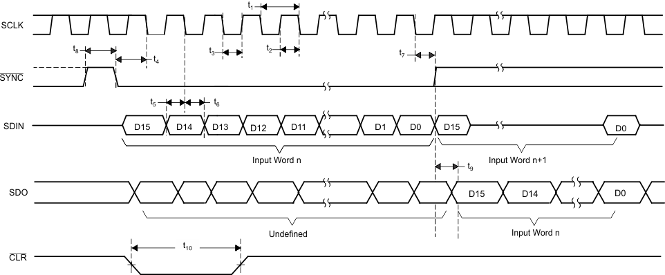 Figure 1. Serial Write Operation Timing Diagram
6.7 Typical Characteristics
At TA = 25°C, unless otherwise noted.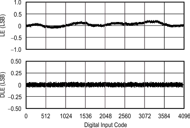
| VDD = 5 V | VREFH = 4.096 V | VREFL = GND |
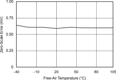
| VDD = 5 V | VREFH = 4.096 V | VREFL = GND |
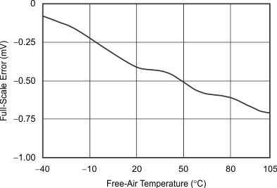
| VDD = 5 V | VREFH = 4.096 V | VREFL = GND |
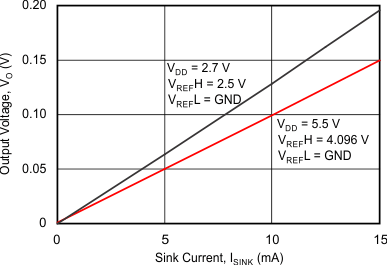
| DAC loaded with 0000h | ||
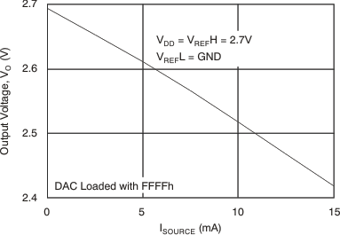
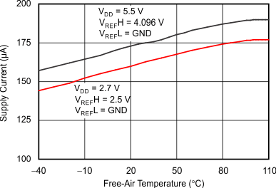
| Powered | No load |
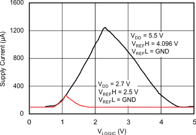
| TA = 25°C | SCLK input | All other inputs = GND |
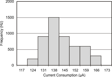
| Digital input code = 2048 | ||
| VDD = 2.7 V | VREFH = 2.5 V | VREFL = GND |
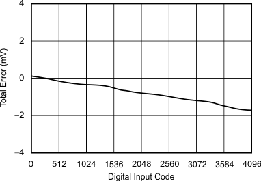
| VDD = 2.7 V | VREFH = 2.5 V | VREFL = GND |
| TA = 25°C |
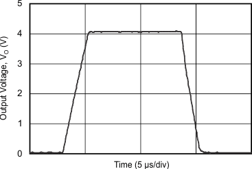
| Output loaded with 200 pF to GND | ||
| Code 0041 to 4055 | ||
| VDD = 5 V | VREFH = 4.096 V | VREFL = GND |
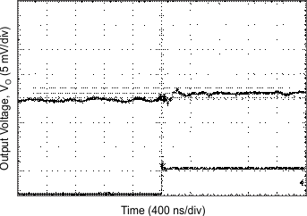
| VDD = 2.7 V | VREFH = 2.5 V | VREFL = GND |
| VDD = 2.7 V | VREFH = 2.5 V | VREFL = GND |
| VDD = 2.7 V | VREFH = 2.5 V | VREFL = GND |
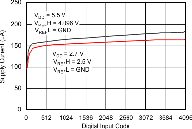
| Powered | No load | |
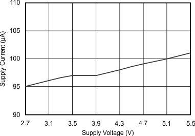
| DAC powered, no load | VREFH = 2.5 V | VREFL = GND |
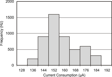
| Digital input code = 2048 | ||
| VDD = 5.5 V | VREFH = 4.096 V | VREFL = GND |
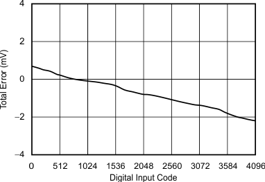
| VDD = 5 V | VREFH = 4.096 V | VREFL = GND |
| TA = 25°C |
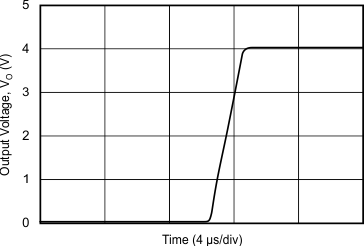
| Power-up code = 4000 | ||
| VDD = 5 V | VREFH = 4.096 V | VREFL = GND |
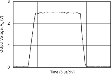
| Output loaded with 200 pF to GND | ||
| Code 0041 to 4055 | ||
| VDD = 2.7 V | VREFH = 2.5 V | VREFL = GND |
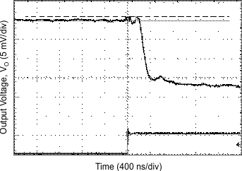
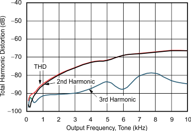
| VDD = 5.5 V | VREFH = 4.096 V | VREFL = GND | |
| fS = 1 MSPS | –1-dB FSR digital input | ||
| Measurement bandwidth = 20 kHz | |||