SLAS950A May 2013 – June 2015 DAC7562-Q1 , DAC7563-Q1 , DAC8162-Q1 , DAC8163-Q1 , DAC8562-Q1 , DAC8563-Q1
PRODUCTION DATA.
- 1 Features
- 2 Applications
- 3 Description
- 4 Revision History
- 5 Device Comparison Table
- 6 Pin Configuration and Functions
- 7 Specifications
- 8 Detailed Description
- 9 Application and Implementation
- 10Power Supply Recommendations
- 11Layout
- 12Device and Documentation Support
- 13Mechanical, Packaging, and Orderable Information
9 Application and Implementation
NOTE
Information in the following applications sections is not part of the TI component specification, and TI does not warrant its accuracy or completeness. TI’s customers are responsible for determining suitability of components for their purposes. Customers should validate and test their design implementation to confirm system functionality.
9.1 Application Information
9.1.1 DAC Internal Reference
The internal reference of the DAC756x-Q1, DAC816x-Q1, and DAC856x-Q1 devices does not require an external load capacitor for stability because it is stable without any capacitive load. However, for improved noise performance, an external load capacitor of 150 nF or larger connected to the VREFIN/VREFOUT output is recommended. Figure 94 shows the typical connections required for operation of the DAC756x-Q1, DAC816x-Q1, and DAC856x-Q1 internal reference. A supply bypass capacitor at the AVDD input is also recommended.
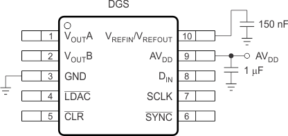 Figure 94. Typical Connection for Operating the DAC756x-Q1, DAC816x-Q1, and DAC856x-Q1 Internal Reference
9.1.1.1 Supply Voltage
The internal reference features an extremely low dropout voltage. It can be operated with a supply of only 5 mV above the reference output voltage in an unloaded condition. For loaded conditions, see the Load Regulation section. The stability of the internal reference with variations in supply voltage (line regulation, dc PSRR) is also exceptional. Within the specified supply voltage range of 2.7 V to 5.5 V, the variation at VREFIN/VREFOUT is typically 50 μV/V; see Figure 7.
9.1.1.2 Temperature Drift
The internal reference is designed to exhibit minimal drift error, defined as the change in reference output voltage over varying temperature. The drift is calculated using the box method described by Equation 3:

where:
VREF_MAX = maximum reference voltage observed within temperature range TRANGE.
VREF_MIN = minimum reference voltage observed within temperature range TRANGE.
VREF = 2.5 V, target value for reference output voltage.
TRANGE = the characterized range from –40°C to 125°C (165°C range)
The internal reference features an exceptional typical drift coefficient of 4 ppm/°C from –40°C to 125°C. Characterizing a large number of units, a maximum drift coefficient of 10 ppm/°C is observed. Temperature drift results are summarized in Figure 3.
9.1.1.3 Noise Performance
Typical 0.1-Hz to 10-Hz voltage noise and noise spectral density performance are listed in the Electrical Characteristics. Additional filtering can be used to improve output noise levels, although care should be taken to ensure the output impedance does not degrade the ac performance. The output noise spectrum at the VREFIN/VREFOUT pin, both unloaded and with an external 4.7-µF load capacitor, is shown in Figure 6. Internal reference noise impacts the DAC output noise when the internal reference is used.
9.1.1.4 Load Regulation
Load regulation is defined as the change in reference output voltage as a result of changes in load current. The load regulation of the internal reference is measured using force and sense contacts as shown in Figure 95. The force and sense lines reduce the impact of contact and trace resistance, resulting in accurate measurement of the load regulation contributed solely by the internal reference. Measurement results are shown in Figure 4. Force and sense lines should be used for applications that require improved load regulation.
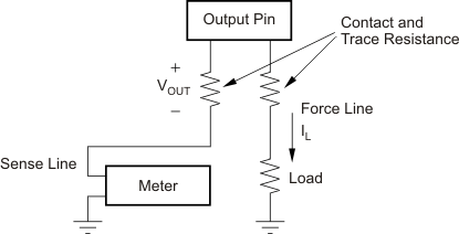 Figure 95. Accurate Load Regulation of the DAC756x-Q1, DAC816x-Q1, and DAC856x-Q1 Internal Reference
9.1.1.4.1 Long-Term Stability
Long-term stability or aging refers to the change of the output voltage of a reference over a period of months or years. This effect lessens as time progresses. The typical drift value for the internal reference is listed in the Electrical Characteristics and measurement results are shown in Figure 5. This parameter is characterized by powering up multiple devices and measuring them at regular intervals.
9.1.1.5 Thermal Hysteresis
Thermal hysteresis for a reference is defined as the change in output voltage after operating the device at 25°C, cycling the device through the operating temperature range, and returning to 25°C. Hysteresis is expressed by Equation 4:

where:
VHYST = thermal hysteresis.
VREF_PRE = output voltage measured at 25°C pre-temperature cycling.
VREF_POST = output voltage measured after the device cycles through the temperature range of –40°C to
aaa 125°C, and returns to 25°C.
VREF_NOM = 2.5 V, target value for reference output voltage.
9.1.2 DAC Noise Performance
Output noise spectral density at the VOUT-n pin versus frequency is depicted in Figure 45 and Figure 46 for full-scale, mid-scale, and zero-scale input codes. The typical noise density for mid-scale code is 90 nV/√Hz at 1 kHz. High-frequency noise can be improved by filtering the reference noise. Integrated output noise between 0.1 Hz and 10 Hz is close to 2.5 µVPP (mid-scale), as shown in Figure 47.
9.2 Typical Applications
9.2.1 Combined Voltage and Current Analog Output Module Using the XTR300
The design features two independent outputs that can source and sink voltage and current over the standard industrial output ranges. The possible outputs of the design include: –24 mA to 24 mA, 4 mA–20 mA, 0 mA to 24 mA, 0 V to 5 V, 0 V to 10 V, –5 V to5 V, and –10 V to 10 V.
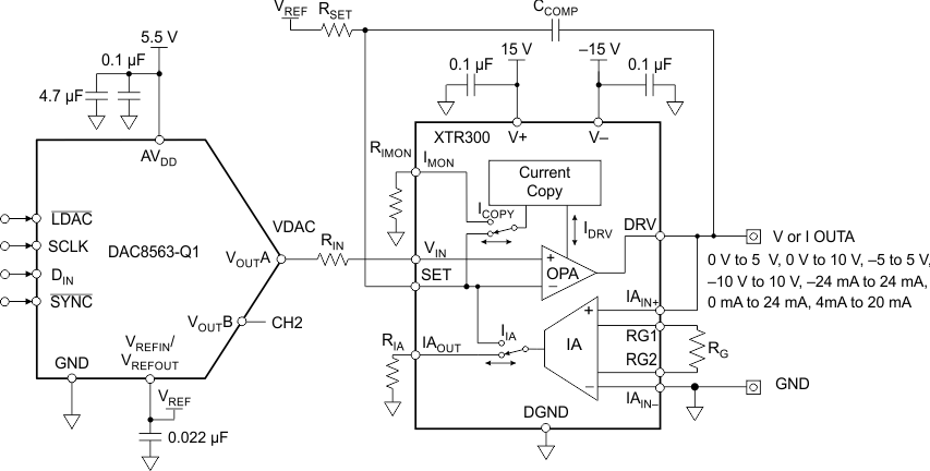 Figure 96. DAC8563-Q1 and XTR300 Discrete Analog Output Module
9.2.1.1 Design Requirements
The design uses a DAC and a current-or-voltage output driver to create a discrete analog output design that can output either voltage or current from the same pin while focusing on high-accuracy specifications. The choice of the DAC8563-Q1 device takes advantage of its 16-bit resolution as well as its low typical offset error of 1 mV and gain error of 0.01% FSR. The choice of the XTR300 device is based on its strong dc performance, having a typical error of 400 µV and 0.04% FSR gain error. The XTR300 device allows a variety of both current and voltage outputs on the same pin while providing load monitoring and error status pins.
The power-on reset-to-midscale feature of the DAC8563-Q1 makes the bipolar output of the XTR300 power up at 0 V or 0 A. If using a unipolar output, the recommended device to achieve a system power-on output of 0 V, 0 A or 4 mA is the DAC8562-Q1 device.
A recommendation for minimizing the introduction of errors into the system is to use ±0.01% tolerance RG and RSET resistors. The bypass capacitors on AVDD, VREF, V+ and V– should have values between 100 nF and 10 µF. Smaller capacitors filter fast low-energy transients, whereas the large capacitors filter the slow high-energy transients. If there is an expectation of both types of signals in the system, the recommendation is to use a pair of small and large values as shown on the AVDD pin of the DAC8563-Q1 device in Figure 96.
9.2.1.2 Detailed Design Procedure
When configured for voltage mode, the output of the instrumentation amplifier (IA), internal to the XTR300 device, is routed to the SET pin. The SET output provides feedback for the IA based on the IA input voltage. The feedback from the IA provides high-impedance remote sensing of the voltage at the output load. Using the output voltage can overcome errors from PCB traces and protection component impedances. The DAC provides a unipolar input voltage to the VIN pin of the XTR300 device. The XTR300 device offsets the VDAC range by a negative VREF and amplifies the difference by a value set by the RG and RSET resistors, as shown in Equation 5.

When configured for current mode, the XTR300 routes the internal output of its current copy circuitry to the SET pin. This provides feedback for the internal OPA driver based on 1 / 10th of the output current, resulting in a voltage-to-current transfer function. Generating bipolar current outputs from the single-ended DAC output voltage, VDAC, requires the application of an offset to the XTR300 SET pin. Connect the RSET resistor from the SET pin to VREF to apply the offset and obtain the transfer function shown in Equation 6.

The desired output ranges for VDAC and VREF voltages determine the RSET and RG resistor values, calculated using Equation 7 and Equation 8. The system design requires a VDAC voltage range of 0.04 V to 4.96 V in order to operate the DAC8563-Q1 in the specified linear output range from codes 512 to 65 024.


IMON and IAOUT accomplish load monitoring. The sizing of RIMON and RIA determine the monitoring output voltage across the resistors. Size the resistors according to Equation 9 and Equation 10 and the expected output load current IDRV.


For more detailed information about the design procedure of this circuit and how to isolate it, see Two-Channel Source/Sink Combined Voltage & Current Output, Isolated, EMC/EMI Tested Reference Design (TIDU434).
9.2.1.3 Application Curves
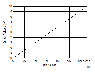
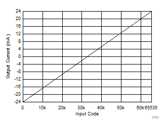
Figure 97 shows the transfer function for the bipolar ±10 V voltage range. This design also supports output voltage ranges of 0–5 V, 0–10 V and ±5 V. Figure 98 shows the transfer function for the unipolar 0–24 mA current range. This design also supports output current ranges of ±24 mA and 4 mA–20 mA.
9.2.2 Up to ±15-V Bipolar Output Using the DAC8562-Q1
The DAC8562-Q1 is designed to be operate from a single power supply providing a maximum output range of AVDD volts. However, the DAC can be placed in the configuration shown in Figure 99 in order to be designed into bipolar systems. Depending on the ratio of the resistor values, the output of the circuit can range anywhere from ±5 V to ±15 V. The design example below shows that the DAC is configured to have its internal reference enabled and the DAC8562-Q1 internal gain set to 2, however, an external 2.5-V reference could also be used (with DAC8562-Q1 internal gain set to 2).
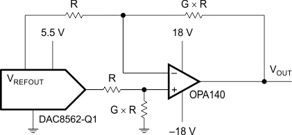 Figure 99. Bipolar Output Range Circuit Using DAC8562-Q1
The transfer function shown in Equation 5 can be used to calculate the output voltage as a function of the DAC code, reference voltage and resistor ratio:

where:
DIN = decimal equivalent of the binary code that is loaded to the DAC register, ranging from 0 to 65,535 for DAC8562-Q1 (16 bit).
VREFOUT = reference output voltage with the internal reference enabled from the DAC VREFIN/VREFOUT pin
G = ratio of the resistors
An example configuration to generate a ±10-V output range is shown below in Equation 6 with G = 4 and VREFOUT = 2.5 V:

In this example, the range is set to ±10 V by using a resistor ratio of four, VREFOUT of 2.5 V, and DAC8562-Q1 internal gain of 2. The resistor sizes must be selected keeping in mind the current sink or source capability of the DAC8562-Q1 internal reference. Using larger resistor values, for example, R = 10 kΩ or larger, is recommended. The op amp is selectable depending on the requirements of the system.
The DAC8562EVM and DAC7562EVM boards have the option to evaluate the bipolar output application by installing the components on the pre-placed footprints. For more information see either the DAC8562EVM or DAC7562EVM product folder.
9.3 System Examples
9.3.1 MSP430 Microprocessor Interfacing
Figure 100 shows a serial interface between the DAC756x-Q1, DAC816x-Q1, or DAC856x-Q1 device and a typical MSP430 USI port such as the one found on the MSP430F2013. The port is configured in SPI master mode by setting bits 3, 5, 6, and 7 in USICTL0. The USI counter interrupt is set in USICTL1 to provide an efficient means of SPI communication with minimal software overhead. The serial clock polarity, source, and speed are controlled by settings in the USI clock control register (USICKCTL). The SYNC signal is derived from a bit-programmable pin on port 1; in this case, port line P1.4 is used. When data are to be transmitted to the DAC756x-Q1, DAC816x-Q1, or DAC856x-Q1 device, P1.4 is taken low. The USI transmits data in 8-bit bytes; thus, only eight falling clock edges occur in the transmit cycle. To load data to the DAC, P1.4 is left low after the first eight bits are transmitted; then, a second write cycle is initiated to transmit the second byte of data. P1.4 is taken high following the completion of the third write cycle.
 Figure 100. DAC756x-Q1, DAC816x-Q1, or DAC856x-Q1 Device to MSP430 Interface
9.3.2 TMS320 McBSP Microprocessor Interfacing
Figure 101 shows an interface between the DAC756x-Q1, DAC816x-Q1, or DAC856x-Q1 device and any TMS320 series DSP from Texas Instruments with a multi-channel buffered serial port (McBSP). Serial data are shifted out on the rising edge of the serial clock and are clocked into the DAC756x-Q1, DAC816x-Q1, or DAC856x-Q1 device on the falling edge of the SCLK signal.
 Figure 101. DAC756x-Q1, DAC816x-Q1, or DAC856x-Q1 Device to TMS320 McBSP Interface
9.3.3 OMAP-L1x Processor Interfacing
Figure 102 shows a serial interface between the DAC756x-Q1, DAC816x-Q1, or DAC856x-Q1 device and the OMAP-L138 processor. The transmit clock CLKx0 of the L138 drives SCLK of the DAC756x-Q1, DAC816x-Q1, or DAC856x-Q1 device, and the data transmit (Dx0) output drives the serial data line of the DAC. The SYNC signal is derived from the frame sync transmit (FSx0) line, similar to the TMS320 interface.
 Figure 102. DAC756x-Q1, DAC816x-Q1, or DAC856x-Q1 Device to OMAP-L1x Processor