JAJSEF2D June   2013  – December 2021 DAC7760 , DAC8760

PRODUCTION DATA  

  1. 特長
  2. アプリケーション
  3. 概要
  4. Revision History
  5. Device Comparison Table
  6. Pin Configuration and Functions
  7. Specifications
    1. 7.1  Absolute Maximum Ratings
    2. 7.2  ESD Ratings
    3. 7.3  Recommended Operating Conditions
    4. 7.4  Thermal Information
    5. 7.5  Electrical Characteristics
    6. 7.6  Electrical Characteristics: AC
    7. 7.7  Timing Requirements: Write Mode
    8. 7.8  Timing Requirements: Readback Mode
    9. 7.9  Timing Diagrams
    10. 7.10 Typical Characteristics
  8. Detailed Description
    1. 8.1 Overview
    2. 8.2 Functional Block Diagram
    3. 8.3 Feature Description
      1. 8.3.1  DAC Architecture
      2. 8.3.2  Voltage Output Stage
      3. 8.3.3  Current Output Stage
      4. 8.3.4  Internal Reference
      5. 8.3.5  Digital Power Supply
      6. 8.3.6  DAC Clear
      7. 8.3.7  Power-On Reset
      8. 8.3.8  Alarm Detection
      9. 8.3.9  Watchdog Timer
      10. 8.3.10 Frame Error Checking
      11. 8.3.11 User Calibration
      12. 8.3.12 Programmable Slew Rate
    4. 8.4 Device Functional Modes
      1. 8.4.1 Setting Voltage and Current Output Ranges
      2. 8.4.2 Boost Configuration for IOUT
      3. 8.4.3 Filtering the Current Output (only on the VQFN package)
      4. 8.4.4 HART Interface
        1. 8.4.4.1 For 4-mA to 20-mA Mode
        2. 8.4.4.2 For All Current Output Modes
    5. 8.5 Programming
      1. 8.5.1 Serial Peripheral Interface (SPI)
        1. 8.5.1.1 SPI Shift Register
        2. 8.5.1.2 Write Operation
        3. 8.5.1.3 Read Operation
        4. 8.5.1.4 Stand-Alone Operation
        5. 8.5.1.5 Multiple Devices on the Bus
    6. 8.6 Register Maps
      1. 8.6.1 DACx760 Command and Register Map
        1. 8.6.1.1 DACx760 Register Descriptions
          1. 8.6.1.1.1 Control Register
          2. 8.6.1.1.2 Configuration Register
          3. 8.6.1.1.3 DAC Registers
          4. 8.6.1.1.4 Reset Register
          5. 8.6.1.1.5 Status Register
  9. Application and Implementation
    1. 9.1 Application Information
      1. 9.1.1 Controlling the VOUT and IOUT Pins
        1. 9.1.1.1 VOUT and IOUT Pins are Independent Outputs, Never Simultaneously Enabled
        2. 9.1.1.2 VOUT and IOUT Pins are Independent Outputs, Simultaneously Enabled
        3. 9.1.1.3 VOUT and IOUT Pins are Tied Together, Never Simultaneously Enabled
      2. 9.1.2 Implementing HART in All Current Output Modes
        1. 9.1.2.1 Using CAP2 Pin on VQFN Package
        2. 9.1.2.2 Using the ISET-R Pin
      3. 9.1.3 Short-Circuit Current Limiting
    2. 9.2 Typical Application
      1. 9.2.1 Design Requirements
      2. 9.2.2 Detailed Design Procedure
      3. 9.2.3 Application Curves
  10. 10Power Supply Recommendations
  11. 11Layout
    1. 11.1 Layout Guidelines
      1. 11.1.1 Thermal Considerations
    2. 11.2 Layout Example
  12. 12Device and Documentation Support
    1. 12.1 Documentation Support
      1. 12.1.1 Related Documentation
    2. 12.2 Receiving Notification of Documentation Updates
    3. 12.3 サポート・リソース
    4. 12.4 Trademarks
    5. 12.5 Electrostatic Discharge Caution
    6. 12.6 Glossary
  13. 13Mechanical, Packaging, and Orderable Information

パッケージ・オプション

メカニカル・データ(パッケージ|ピン)
サーマルパッド・メカニカル・データ
発注情報

Detailed Design Procedure

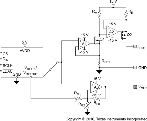
GUID-180E472E-AA37-499D-8977-7CA80AFCBD03-low.gifFigure 9-7 Generic Design for Typical PLC Current and Voltage Outputs

Figure 9-7 illustrates a common generic solution for realizing these desired voltage and current output spans.

The current output circuit is comprised of amplifiers A1 and A2, MOSFETs Q1 and Q1, and the three resistors RSET, RA, and RB. This two-stage current source enables the ground-referenced DAC output voltage to drive the high-side amplifier required for the current-source.

The voltage output circuit is composed of amplifier A3 and the resistor network consisting of RFB, RG1, and RG2. A3 operates as a modified summing amplifier, where the DAC controls the noninverting input and the inverting input has one path to GND and a second to VREF. This configuration allows the single-ended DAC to create both the unipolar 0-V to 5-V and 0-V to 10-V outputs and the bipolar ±5-V and ±10-V outputs by modifying the values of RG1 and RG2.

Figure 9-6 generates clean ±15-V supplies using a synchronous step-down regulator (TPS54062) and two high-voltage, ultra-low noise, linear regulators (TPS7A49 and TPS7A30). A field supply terminal is shown instead of the more common use case of a back-plane supply. The design uses two triple channel isolators (ISO7631FC) to provide galvanic isolation for the digital lines to communicate to the main controller. Note that these isolators can be driven by the internally-generated supply (DVDD) from the DACx760 to save components and cost. The DACx760 supplies up to 10 mA that meets the supply requirements of the two isolators running at up to 10 Mbps. Note that additional cost savings are possible if noncritical digital signals such as CLR and ALARM are tied to GND or left unconnected. Finally, a protection scheme with transient voltage suppressors and other components is placed on all pins which connect to the field.

The protection circuitry is designed to provide immunity to the IEC61000-4 test suite which includes system-level industrial transient tests. The protection circuit includes transient voltage suppressor (TVS) diodes, clamp-to-rail steering diodes, and pass elements in the form of resistors and ferrite beads. For more detail about selecting these components, see TIPD153.