JAJSCW9 February 2017 DAC8775
PRODUCTION DATA.
- 1 特長
- 2 アプリケーション
- 3 概要
- 4 改訂履歴
- 5 Device Comparison Table
- 6 Pin Configuration and Functions
- 7 Specifications
-
8 Detailed Description
- 8.1 Overview
- 8.2 Functional Block Diagram
- 8.3
Feature Description
- 8.3.1 Current Output Stage
- 8.3.2 Voltage Output Stage
- 8.3.3 Buck-Boost Converter
- 8.3.4 Analog Power Supply
- 8.3.5 Digital Power Supply
- 8.3.6 Internal Reference
- 8.3.7 Power-On-Reset
- 8.3.8 ALARM Pin
- 8.3.9 Power GOOD Bits
- 8.3.10 Status Register
- 8.3.11 Status Mask
- 8.3.12 Alarm Action
- 8.3.13 Watchdog Timer
- 8.3.14 Programmable Slew Rate
- 8.3.15 HART Interface
- 8.4 Device Functional Modes
- 8.5
Register Maps
- 8.5.1 DAC8775 Commands
- 8.5.2
Register Maps and Bit Functions
- 8.5.2.1 No Operation Register (address = 0x00) [reset = 0x0000]
- 8.5.2.2 Reset Register (address = 0x01) [reset = 0x0000]
- 8.5.2.3 Reset Config Register (address = 0x02) [reset = 0x0000]
- 8.5.2.4 Select DAC Register (address = 0x03) [reset = 0x0000]
- 8.5.2.5 Configuration DAC Register (address = 0x04) [reset = 0x0000]
- 8.5.2.6 DAC Data Register (address = 0x05) [reset = 0x0000]
- 8.5.2.7 Select Buck-Boost Converter Register (address = 0x06) [reset = 0x0000]
- 8.5.2.8 Configuration Buck-Boost Register (address = 0x07) [reset = 0x0000]
- 8.5.2.9 DAC Channel Calibration Enable Register (address = 0x08) [reset = 0x0000]
- 8.5.2.10 DAC Channel Gain Calibration Register (address = 0x09) [reset = 0x0000]
- 8.5.2.11 DAC Channel Offset Calibration Register (address = 0x0A) [reset = 0x0000]
- 8.5.2.12 Status Register (address = 0x0B) [reset = 0x1000]
- 8.5.2.13 Status Mask Register (address = 0x0C) [reset = 0x0000]
- 8.5.2.14 Alarm Action Register (address = 0x0D) [reset = 0x0000]
- 8.5.2.15 User Alarm Code Register (address = 0x0E) [reset = 0x0000]
- 8.5.2.16 Reserved Register (address = 0x0F) [reset = N/A]
- 8.5.2.17 Write Watchdog Timer Register (address = 0x10) [reset = 0x0000]
- 8.5.2.18 Device ID Register (address = 0x11) [reset = 0x0000]
- 8.5.2.19 Reserved Register (address 0x12 - 0xFF) [reset = N/A]
- 9 Application and Implementation
- 10Power Supply Recommendations
- 11Layout
- 12デバイスおよびドキュメントのサポート
- 13メカニカル、パッケージ、および注文情報
- 14メカニカル、パッケージ、および注文情報
10 Power Supply Recommendations
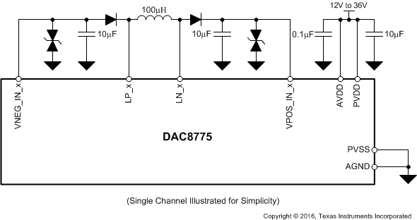
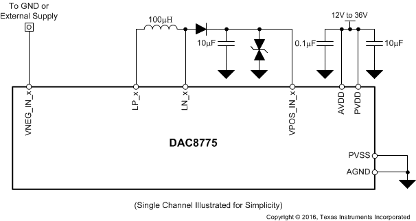
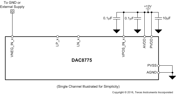
There are three possible hardware power supply configurations for the DAC8775: the internal DC/DC provides both positive and negative supply voltages, the internal DC/DC provides only one of the supply voltages with an external supply provided on the other, or the internal DC/DC is not used at all and external supply voltages are provided for both positive and negative supply voltages. Simple illustrations for each case are shown below.
 Figure 135. DAC8775 With Dual Supplies from Internal DC/DC
Figure 136 illustrates using a single supply from the DAC8775 internal DC/DC and the other supply from an external source. In this example the VNEG_IN_x supply is the input being supplied by an external supply, or ground for unipolar output spans. A similar scheme could be used if VPOS_IN_x was supplied by an external supply and VNEG_IN_x was supplied by the internal DC/DC.
 Figure 136. DAC8775 With Single Supply from Internal DC/DC
The scheme in Figure 137 should be used if the internal DC/DC is not used at all and external supplies are selected for VPOS_IN_x and VNEG_IN_x. When using external supplies for VPOS_IN_x it is important that VPOS_IN_x, PVDD, and AVDD nodes are tied to the same voltage potential with the same ramp-rate.
 Figure 137. DAC8775 with External Supplies