JAJS013I December   2000  – September 2020 DCP010505B , DCP010505DB , DCP010507DB , DCP010512B , DCP010512DB , DCP010515B , DCP010515DB , DCP011512DB , DCP011515DB , DCP012405B , DCP012415DB

PRODUCTION DATA  

  1. 特長
  2. アプリケーション
  3. 概要
  4. Revision History
  5. Pin Configuration and Functions
    1.     Pin Functions
  6. Specifications
    1. 6.1 Absolute Maximum Ratings
    2. 6.2 ESD Ratings
    3. 6.3 Recommended Operating Conditions
    4. 6.4 Thermal Information
    5. 6.5 Electrical Characteristics
    6. 6.6 Switching Characteristics
    7. 6.7 Typical Characteristics
  7. Detailed Description
    1. 7.1 Overview
    2. 7.2 Functional Block Diagrams
    3. 7.3 Feature Description
      1. 7.3.1  Isolation
        1. 7.3.1.1 Operation or Functional Isolation
        2. 7.3.1.2 Basic or Enhanced Isolation
        3. 7.3.1.3 Continuous Voltage
        4. 7.3.1.4 Isolation Voltage
        5. 7.3.1.5 Repeated High-Voltage Isolation Testing
      2. 7.3.2  Power Stage
      3. 7.3.3  Oscillator And Watchdog Circuit
      4. 7.3.4  Thermal Shutdown
      5. 7.3.5  Synchronization
      6. 7.3.6  Light Load Operation (< 10%)
      7. 7.3.7  Load Regulation (10% to 100%)
      8. 7.3.8  Construction
      9. 7.3.9  Thermal Management
      10. 7.3.10 Power-Up Characteristics
    4. 7.4 Device Functional Modes
      1. 7.4.1 Disable and Enable (SYNCIN Pin)
      2. 7.4.2 Decoupling
        1. 7.4.2.1 Ripple Reduction
        2. 7.4.2.2 Connecting the DCP01B in Series
        3. 7.4.2.3 Connecting the DCP01B in Parallel
  8. Application and Implementation
    1. 8.1 Application Information
    2. 8.2 Typical Application
      1. 8.2.1 Design Requirements
      2. 8.2.2 Detailed Design Procedure
        1. 8.2.2.1 Input Capacitor
        2. 8.2.2.2 Output Capacitor
        3. 8.2.2.3 SYNCIN Pin
      3. 8.2.3 DCP010505 Application Curves
      4. 8.2.4 PCB Design
      5. 8.2.5 Decoupling Ceramic Capacitors
      6. 8.2.6 Input Capacitor and the Effects of ESR
      7. 8.2.7 Ripple and Noise
        1. 8.2.7.1 Output Ripple Calculation Example
      8. 8.2.8 Dual DCP01B Output Voltage
      9. 8.2.9 Optimizing Performance
  9. Power Supply Recommendations
  10. 10Layout
    1. 10.1 Layout Guidelines
    2. 10.2 Layout Example
  11. 11Device and Documentation Support
    1. 11.1 Device Support
      1. 11.1.1 Device Nomenclature
    2. 11.2 Documentation Support
      1. 11.2.1 Related Documentation
    3. 11.3 Receiving Notification of Documentation Updates
    4. 11.4 Support Resources
    5. 11.5 Trademarks
    6. 11.6 Glossary
    7. 11.7 Electrostatic Discharge Caution
  12. 12Mechanical, Packaging, and Orderable Information

パッケージ・オプション

メカニカル・データ(パッケージ|ピン)
サーマルパッド・メカニカル・データ
発注情報

Connecting the DCP01B in Series

Multiple DCP01B isolated 1-W DC/DC converters can be connected in series to provide non-standard voltage rails. This configuration is possible by using the floating outputs provided by the galvanic isolation of the DCP01.

Connect the +VOUT from one DCP01B to the –VOUT of another (see Figure 7-6). If the SYNCIN pins are tied together, the self-synchronization feature of the DCP01B prevents beat frequencies on the voltage rails. The synchronization feature of the DCP01B allows easy series connection without external filtering, thus minimizing cost.
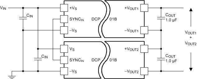
GUID-86197989-CEA9-4D4B-8AF4-F7A83FAA553A-low.gifFigure 7-6 Multiple DCP01B Devices Connected in Series

The outputs of a dual-output DCP01B can also be connected in series to provide two times the magnitude of +VOUT, as shown in Figure 7-7. For example, connect a dual-output, 15-V, DCP012415DB device to provide a 30-V rail.

GUID-D509DC91-5C0D-429E-9219-5D207EAAA1BD-low.gifFigure 7-7 Dual Output Devices Connected in Series