JAJSD60 April 2017 DCPA10505 , DCPA10505D , DCPA10512 , DCPA10512D , DCPA10515 , DCPA10515D
PRODUCTION DATA.
- 1 特長
- 2 アプリケーション
- 3 概要
- 4 改訂履歴
- 5 Pin Configuration and Functions
-
6 Specifications
- 6.1 Absolute Maximum Ratings
- 6.2 ESD Ratings
- 6.3 Recommended Operating Conditions
- 6.4 Electrical Characteristics
- 6.5 Switching Characteristics
- 6.6 Typical Characteristics (DCPA10505)
- 6.7 Typical Characteristics (DCPA10512)
- 6.8 Typical Characteristics (DCPA10515)
- 6.9 Typical Characteristics (DCPA10505D)
- 6.10 Typical Characteristics (DCPA10512D)
- 6.11 Typical Characteristics (DCPA10515D)
-
7 Detailed Description
- 7.1 Overview
- 7.2 Functional Block Diagrams
- 7.3 Feature Description
- 8 Application and Implementation
- 9 Power Supply Recommendations
- 10Layout
- 11デバイスおよびドキュメントのサポート
- 12メカニカル、パッケージ、および注文情報
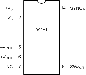
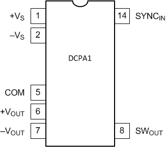
5 Pin Configuration and Functions
NVA and DUA Package
7-Pin PDIP and SOP (Single Output)
(Top View)

NVA and DUA Package
7-Pin PDIP and SOP (Dual Output)
(Top View)

Pin Functions
| PIN NAME | PIN NUMBER | I/O (1) | Description | |
|---|---|---|---|---|
| SINGLE-OUTPUT | DUAL-OUTPUT | |||
| COM | — | 5 | O | Output side common |
| NC | 7 | — | — | No connection |
| SYNCIN | 14 | 14 | I | Synchronization. This pin is used to synchronize to an external clock. Internally it is pulled to GND. If valid clock is not detected on this pin, the SN6505 shifts automatically to internal clock. |
| SWOUT | 8 | 8 | O | Unrectified transformer output. |
| +VOUT | 6 | 6 | O | Positive output voltage |
| +VS | 1 | 1 | I | Input voltage |
| –VOUT | 5 | 7 | O | Negative output voltage |
| –VS | 2 | 2 | I | Input side common |
(1) I = Input, O = Output