JAJSMN8D December   2000  – August 2021 DCR021205 , DCR022405

PRODUCTION DATA  

  1. 特長
  2. アプリケーション
  3. 概要
  4. Revision History
  5. Pin Configuration and Functions
  6. Specifications
    1. 6.1 Absolute Maximum Ratings
    2. 6.2 ESD Ratings
    3. 6.3 Recommended Operating Conditions
    4. 6.4 Thermal Information
    5. 6.5 Electrical Characteristics
    6. 6.6 Typical Characteristics
  7. Detailed Description
    1. 7.1 Overview
    2. 7.2 Functional Block Diagram
    3. 7.3 Feature Description
      1. 7.3.1 Isolation
        1. 7.3.1.1 Operation or Functional Isolation
        2. 7.3.1.2 Basic or Enhanced Isolation
        3. 7.3.1.3 Working Voltage
        4. 7.3.1.4 Isolation Voltage Rating
        5. 7.3.1.5 Repeated High-Voltage Isolation Testing
      2. 7.3.2 Power Stage
      3. 7.3.3 Oscillator and Watchdog
      4. 7.3.4 ERROR Flag
      5. 7.3.5 Synchronization
      6. 7.3.6 Construction
      7. 7.3.7 Decoupling – Ripple Reduction
    4. 7.4 Device Functional Modes
      1. 7.4.1 Device Disable and Enable
      2. 7.4.2 Regulated Output Disable and Enable
  8. Application and Implementation
    1. 8.1 Application Information
      1. 8.1.1 DCR02 Single Voltage Output
      2. 8.1.2 Generating Two Positive Output Voltages
      3. 8.1.3 Generation of Dual Polarity Voltages from Two Self-Synchronized DCR02s
    2. 8.2 Typical Application
      1. 8.2.1 Design Requirements
      2. 8.2.2 Detailed Design Procedure
        1. 8.2.2.1 Input Capacitor
        2. 8.2.2.2 Output Capacitor
        3. 8.2.2.3 Filter Capacitor
        4. 8.2.2.4 ERROR Flag
      3. 8.2.3 Application Curves
  9. Power Supply Recommendations
  10. 10Layout
    1. 10.1 Layout Guidelines
    2. 10.2 Layout Examples
    3. 10.3 Thermal Consideration
  11. 11Device and Documentation Support
    1. 11.1 Documentation Support
      1. 11.1.1 Related Documentation
    2. 11.2 Receiving Notification of Documentation Updates
    3. 11.3 サポート・リソース
    4. 11.4 Trademarks
    5. 11.5 Electrostatic Discharge Caution
    6. 11.6 Glossary
  12. 12Mechanical, Packaging, and Orderable Information

パッケージ・オプション

メカニカル・データ(パッケージ|ピン)
サーマルパッド・メカニカル・データ
発注情報

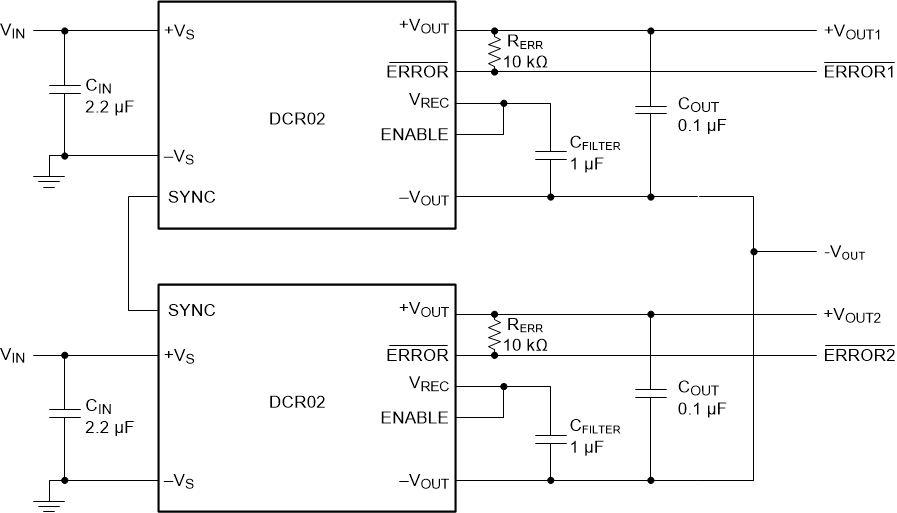
Generating Two Positive Output Voltages

Two DCR02s can be used to create two +5-V output voltages, as shown in Figure 8-2. The two DCR02s are connected in self-synchronization, thus locking the oscillators of both devices to a single frequency. The ERROR and ENABLE facilities can be used in a similar configuration for a single DCR02. The filter capacitors connected to the VREC pins (CFILTER) must be kept separate from each other and connected in close proximity to the respective DCR02. If similar output voltages are being used, TI does not recommend that a single filter capacitor (with an increased capacitance) be used with both VREC pins connected together, because this could result in the overloading of one of the devices.
GUID-6E641737-5AE6-4ADE-B3A0-221988C25AD8-low.gif
Low-ESR, ceramic capacitors are required for CIN, COUT, and CFILTER.
Figure 8-2 Generating Two Positive Voltages from Self-Synchronized DCR02s