JAJSHA6B March 2019 – May 2022 DLP2000
PRODUCTION DATA
- 1 特長
- 2 アプリケーション
- 3 概要
- 4 Revision History
- 5 Pin Configuration and Functions
-
6 Specifications
- 6.1 Absolute Maximum Ratings
- 6.2 Storage Conditions
- 6.3 ESD Ratings
- 6.4 Recommended Operating Conditions
- 6.5 Thermal Information
- 6.6 Electrical Characteristics
- 6.7 Timing Requirements
- 6.8 System Mounting Interface Loads
- 6.9 Physical Characteristics of the Micromirror Array
- 6.10 Micromirror Array Optical Characteristics
- 6.11 Window Characteristics
- 6.12 Chipset Component Usage Specification
- 7 Detailed Description
- 8 Application and Implementation
- 9 Power Supply Recommendations
- 10Layout
- 11Device and Documentation Support
- 12Mechanical, Packaging, and Orderable Information
6.4 Recommended Operating Conditions
Over operating free-air temperature range (unless otherwise noted)
| MIN | NOM | MAX | UNIT | |||
|---|---|---|---|---|---|---|
| Supply Voltage | VCC | LVCMOS logic power supply voltage(1) | 1.65 | 1.8 | 1.95 | V |
| VOFFSET | Mirror electrode and HVCMOS voltage(1) | 8.25 | 8.5 | 8.75 | V | |
| VBIAS | Mirror electrode voltage | 15.5 | 16 | 16.5 | V | |
| Supply voltage delta |VBIAS – VOFFSET| (2) | 8.75 | V | ||||
| VRESET | Mirror electrode voltage | –9.5 | –10 | –10.5 | V | |
| Input Voltage | VP | Positive going threshold voltage | 0.4*VCC | 0.7*VCC | V | |
| VN | Negative going threshold voltage | 0.3*VCC | 0.6*VCC | V | ||
| VH | Hysteresis voltage (Vp – Vn) | 0.1*VCC | 0.4*VCC | V | ||
| Environmental | TARRAY | Array temperature—long-term operational(3)(4)(5)(6) | 0 | 40 to 70 | °C | |
| Array Temperature – short-term operational(4)(7) | –20 | 75 | °C | |||
| |TDELTA| | Absolute temperature difference between any point on the window edge and the ceramic test point TP1(8) | 15 | °C | |||
| TWINDOW | Window temperature—operational(3)(9) | 90 | °C | |||
| TDP | Dew point temperature (non-condensing) | See note(10). | °C | |||
| ILLUV | Illumination wavelength < 400 nm(3) | 0.68 | mW/cm2 | |||
| ILLVIS | Illumination wavelengths between 400 nm and 700 nm | Thermally limited | ||||
| ILLIR | Illumination wavelength > 700 nm | 10 | mW/cm2 | |||
(1) All voltage values are with respect to GND (VSS).
VOFFSET, VCC, VBIAS,
VRESET,
and VSS power supplies are required for the normal DMD operating
mode.
(2) To prevent excess current, the supply voltage delta
|VBIAS – VOFFSET| must be less than 8.75 V.
(3) Simultaneous exposure of the DMD to the maximum
Recommended Operating
Conditions
for temperature and UV illumination
reduces
device lifetime.
(4) The array temperature cannot be measured directly and must be
computed analytically from the temperature measured at test point 1 (TP1) shown
in Figure 7-1 and the package thermal resistance
in
Section 7.6.
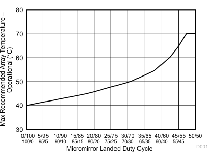
(5) Per Figure 6-1, the maximum operational array temperature should be derated based on the
micromirror landed duty cycle that the DMD experiences in the end application.
Refer to
Section 7.7
for a definition of micromirror landed duty cycle.
(6) Long-term is defined as the usable life of the device
(7) Array temperatures beyond those specified as long-term are
recommended for short-term conditions only (power-up). Short-term is defined as
cumulative time over the usable life of the device and is less than 500 hours
for temperatures between the long-term maximum and 75°C, and less than 500 hours
for temperatures between 0°C and –20°C.
(8) Temperature delta is the highest difference between the
ceramic test point 1 (TP1) and anywhere on the window edge as shown in Figure 7-1.
(9) Window temperature is the highest temperature on the window
edge shown in Figure 7-1.
(10) The DLP2000 DMD is intended for use in well controlled, low dew
point environments. Please contact your local TI sales person or TI distributor
representative to determine if this device is suitable for your application and
operating environment compared other DMD solutions. DLP Products offers a broad
portfolio of DMDs suitable for a wide variety of applications.
 Figure 6-1 Max Recommended Array
Temperature—Derating
Curve