JAJSHA6B March 2019 – May 2022 DLP2000
PRODUCTION DATA
- 1 特長
- 2 アプリケーション
- 3 概要
- 4 Revision History
- 5 Pin Configuration and Functions
-
6 Specifications
- 6.1 Absolute Maximum Ratings
- 6.2 Storage Conditions
- 6.3 ESD Ratings
- 6.4 Recommended Operating Conditions
- 6.5 Thermal Information
- 6.6 Electrical Characteristics
- 6.7 Timing Requirements
- 6.8 System Mounting Interface Loads
- 6.9 Physical Characteristics of the Micromirror Array
- 6.10 Micromirror Array Optical Characteristics
- 6.11 Window Characteristics
- 6.12 Chipset Component Usage Specification
- 7 Detailed Description
- 8 Application and Implementation
- 9 Power Supply Recommendations
- 10Layout
- 11Device and Documentation Support
- 12Mechanical, Packaging, and Orderable Information
6.9 Physical Characteristics of the Micromirror Array
| PARAMETER | VALUE | UNIT | ||
|---|---|---|---|---|
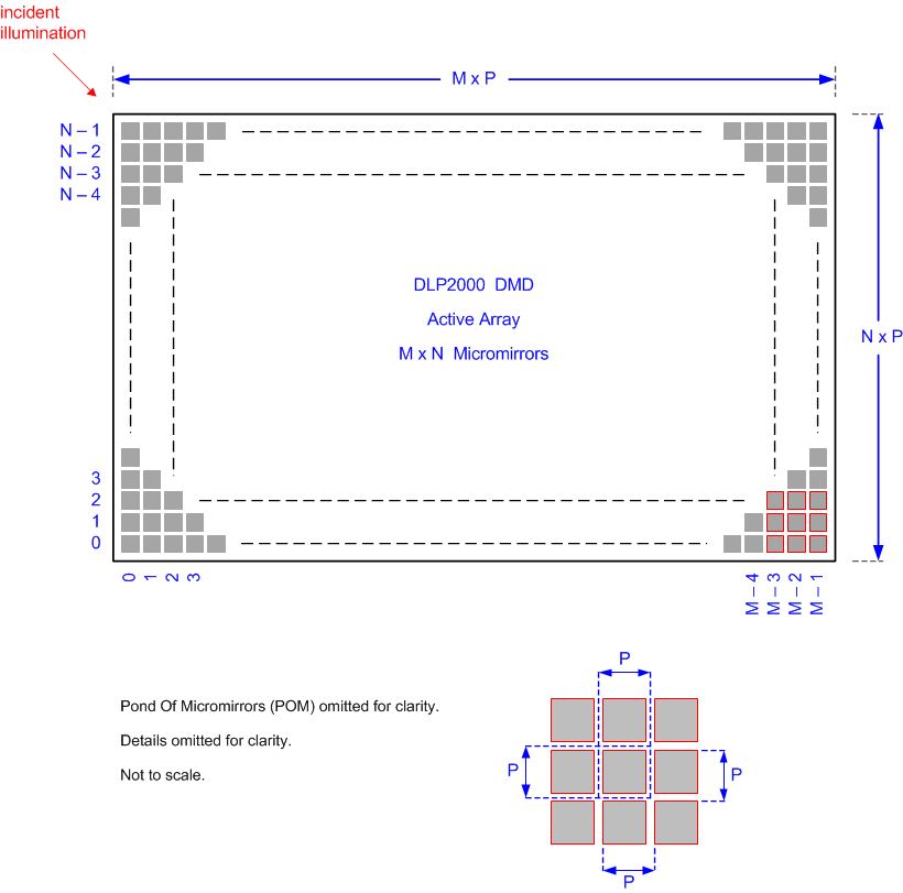
| M | Number of active columns(1) | See Figure 6-8. | 640 | micromirrors |
| N | Number of active rows(1) | See Figure 6-8. | 360 | micromirrors |
| P | Micromirror (pixel) pitch(1) | See Figure 6-8. | 7.56 | µm |
| Micromirror active array width(1) | M × P | 4.8384 | mm | |
| Micromirror active array height(1) | N × P | 2.7216 | mm | |
| Micromirror active border(2)(3) | Pond of micromirrors (POM) | 8 | micromirrors, side | |
(1) See Figure 6-8.
(2) The structure and qualities of the border around the active array include a
band of partially functional micromirrors called the
“pond
of
micromirrors”
(POM). These micromirrors are structurally and/or electrically prevented from
tilting toward the bright or “on” state but still require an electrical bias to
tilt toward “off.”
(3) Out of the
eight
POM rows on the top and bottom, only the
one
POM row closest to the active array is electrically attached to that reset
group. The other
seven
POM rows are attached to a dedicated POM internal reset driver circuit.
 Figure 6-8 Micromirror Array Physical Characteristics