JAJSGU1B January 2019 – May 2022 DLP4500NIR
PRODUCTION DATA
- 1 特長
- 2 アプリケーション
- 3 概要
- 4 Revision History
- 5 Chipset Component Usage Specification
- 6 Pin Configuration and Functions
-
7 Specifications
- 7.1 Absolute Maximum Ratings
- 7.2 Storage Conditions
- 7.3 ESD Ratings
- 7.4 Recommended Operating Conditions
- 7.5 Thermal Information
- 7.6 Electrical Characteristics
- 7.7 Timing Requirements
- 7.8 System Mounting Interface Loads
- 7.9 Micromirror Array Physical Characteristics
- 7.10 Micromirror Array Optical Characteristics
- 7.11 Typical Characteristics
- 8 Detailed Description
- 9 Applications and Implementation
- 10Power Supply Recommendations
-
11Layout
- 11.1 Layout Guidelines
- 11.2 Layout Example
- 12Device and Documentation Support
- 13Mechanical, Packaging, and Orderable Information
7.7 Timing Requirements
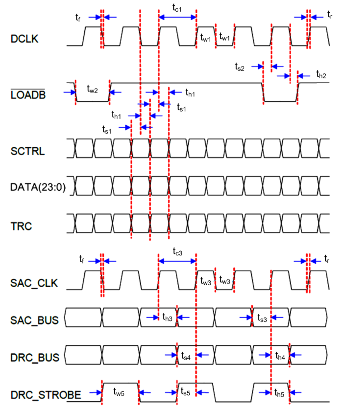
Over operating free-air temperature range (unless otherwise noted). This data sheet provides timing at the device pin.
| MIN | NOM | MAX | UNIT | |||
|---|---|---|---|---|---|---|
| tsu(1) | Setup time: DATA before rising or falling edge of DCLK (1) | 0.7 | ns | |||
| Setup time: TRC before rising or falling edge of DCLK (1) | 0.7 | |||||
| Setup time: SCTRL before rising or falling edge of DCLK (1) | 0.7 | |||||
| tsu(2) | Setup time: LOADB low before rising edge of DCLK (1) | 0.7 | ns | |||
| tsu(3) | Setup time: SAC_BUS low before rising edge of SAC_CLK (1) | 1 | ns | |||
| tsu(4) | Setup time: DRC_BUS high before rising edge of SAC_CLK (1) | 1 | ns | |||
| tsu(5) | Setup time: DRC_STROBE high before rising edge of SAC_CLK (1) | 2 | ns | |||
| th(1) | Hold time: DATA after rising or falling edge of DCLK (1) | 0.7 | ns | |||
| Hold time: TRC after rising or falling edge of DCLK (1) | 0.7 | |||||
| Hold time: SCTRL after rising or falling edge of DCLK (1) | 0.7 | |||||
| th(2) | Hold time: LOADB low after falling edge of DCLK (1) | 0.7 | ns | |||
| th(3) | Hold time: SAC_BUS low after rising edge of SAC_CLK (1) | 1 | ns | |||
| th(4) | Hold time: DRC_BUS after rising edge of SAC_CLK (1) | 1 | ns | |||
| th(5) | Hold time: DRC_STROBE after rising edge of SAC_CLK (1) | 2 | ns | |||
| tr | Rise time (20% to 80%): DCLK / SAC_CLK, VREF = 1.8 V | 1.08 | ns | |||
| Rise time (20% to 80%): DATA / TRC / SCTRL / LOADB, VREF = 1.8 V | 1.08 | |||||
| tf | Fall time (20% to 80%): DCLK / SAC_CLK, VREF = 1.8 V | 1.08 | ns | |||
| Fall time (20% to 80%): DATA / TRC / SCTRL / LOADB | 1.08 | |||||
| tc1 | Clock cycle: DCLK | 8.33 | 10 | 12.5 | ns | |
| tc3 | Clock cycle: SAC_CLK | 12.5 | 13.33 | 14.3 | ns | |
| tw1 | Pulse width high or low: DCLK | 3.33 | ns | |||
| tw2 | Pulse width low: LOADB | 4.73 | ns | |||
| tw3 | Pulse width high or low: SAC_CLK | 5 | ns | |||
| tw5 | Pulse width high: DRC_STROBE | 7 | ns | |||
(1) Setup and hold times shown are for fast input slew rates >1 V/ns. For slow slew rates >0.5 V/ns and <1 V/ns, the setup and hold times are longer. For every 0.1 V/ns decrease in slew rate from 1 V/ns, add 150 ps on setup and hold.
 Figure 7-2 Timing Diagram