JAJSIM4A November 2020 – July 2022 DLP500YX
PRODUCTION DATA
- 1 特長
- 2 アプリケーション
- 3 概要
- 4 Revision History
- 5 Pin Configuration and Functions
-
6 Specifications
- 6.1 Absolute Maximum Ratings
- 6.2 Storage Conditions
- 6.3 ESD Ratings
- 6.4 Recommended Operating Conditions
- 6.5 Thermal Information
- 6.6 Electrical Characteristics
- 6.7 Capacitance at Recommended Operating Conditions
- 6.8 Timing Requirements
- 6.9 Typical Characteristics
- 6.10 System Mounting Interface Loads
- 6.11 Micromirror Array Physical Characteristics
- 6.12 Micromirror Array Optical Characteristics
- 6.13 Window Characteristics
- 6.14 Chipset Component Usage Specification
- 7 Detailed Description
- 8 Application and Implementation
- 9 Power Supply Recommendations
- 10Layout
- 11Device and Documentation Support
- 12Mechanical, Packaging, and Orderable Information
10.1.1 Critical Signal Guidelines
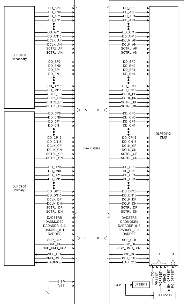
The DLP500YX DMD is one device in a chipset controlled by the DLPC900 Controller. The following guidelines are targeted at designing a functioning PCB using this DLP500YX DMD chipset. The DLP500YX DMD board must be a high-speed multi-layer PCB containing high-speed digital logic utilizing dual edge (DDR) LVDS signals at 400 MHz clock rates. Figure 10-1 shows the DLP500YX signals and the recommendations needed from/to the DLPC900 Controller devices. The DLPC900 device provides the data and control to the DMD. The TPS65145 and LP38513 devices supply power to the DMD.
 Figure 10-1 DLP500YX DMD System Connections and
Layout Restrictions
Figure 10-1 DLP500YX DMD System Connections and
Layout Restrictions| Note | Signal Type | Guideline |
|---|---|---|
| A | Differential | Prevent signal noise |
| Route 100 ±10-Ω resistor | ||
| Intra-pair (P-to-N) length tolerance is ±12-mils | ||
| DD and SCTRL must be matched to the DCLK within ±150-mils | ||
| DCLK_C must be matched to DCLK_D within ±1.25-ns | ||
| DCLK_A must be matched to DCLK_B within ±1.25-ns | ||
| Do not switch routing layers except at the beginning and end of trace | ||
| Signal routing length must not exceed 375-mm | ||
| B | Single-ended | Prevent signal noise |
| Route single-ended signals 50 ±5-Ω | ||
| No length match requirement | ||
| C | Power | VRESET, VOFFSET, VBIAS, and VCC at the DMD must be kept within the operating limits specified in the data sheet |
| Provide proper amount of decoupling capacitance for each voltage at the DMD |