JAJSJA0B July 2020 – April 2021 DLP5530S-Q1
PRODUCTION DATA
- 1 特長
- 2 アプリケーション
- 3 概要
- 4 Revision History
- 5 Pin Configuration and Functions
-
6 Specifications
- 6.1 Absolute Maximum Ratings
- 6.2 Storage Conditions
- 6.3 ESD Ratings
- 6.4 Recommended Operating Conditions
- Illumination Overfill Diagram
- 6.5 Thermal Information
- 6.6 Electrical Characteristics
- 6.7 Timing Requirements
- Electrical and Timing Diagrams
- 6.8 Switching Characteristics
- LPSDR and Test Load Circuit Diagrams
- 6.9 System Mounting Interface Loads
- System Interface Loads Diagram
- 6.10 Physical Characteristics of the Micromirror Array
- Array Physical Characteristics Diagram
- 6.11 Micromirror Array Optical Characteristics
- 6.12 Window Characteristics
- 6.13 Chipset Component Usage Specification
- 7 Detailed Description
- 8 Application and Implementation
- 9 Power Supply Recommendations
- 10Layout
- 11Device and Documentation Support
- 12Mechanical, Packaging, and Orderable Information
パッケージ・オプション
デバイスごとのパッケージ図は、PDF版データシートをご参照ください。
メカニカル・データ(パッケージ|ピン)
- FYS|149
サーマルパッド・メカニカル・データ
発注情報
7.6 Micromirror Array Temperature Calculation
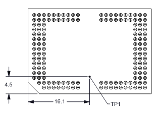
 Figure 7-4 DMD Thermal Test Points
The active array temperature can be computed analytically from measurement points on the outside of the package, the package thermal resistance, the electrical power, and the illumination heat load.
Relationship between array temperature and the reference ceramic temperature (thermocouple location TP1 in Figure 7-4) is provided by the following equations:
where
- TARRAY = computed DMD array temperature (°C)
- TCERAMIC = measured ceramic temperature, TP1 location in Figure 7-4 (°C)
- RARRAY–TO–CERAMIC = DMD package thermal resistance from array to thermal test point TP1 (°C/W), see Thermal Information
- QARRAY = total power, electrical plus absorbed, on the DMD array (W)
- QELECTRICAL = nominal electrical power dissipation by the DMD (W)
- QILLUMINATION = (CL2W × SL)
- CL2W = conversion constant for screen lumens to power on the DMD (W/lm)
- SL = measured screen lumens (lm)
Electrical power dissipation of the DMD is variable and depends on the voltages, data rates, and operating frequencies.
Absorbed power from the illumination source is variable and depends on the operating state of the mirrors and the intensity of the light source.
Equations shown above are valid for a 1–chip DMD system with a total projection efficiency from DMD to the screen of 87%.
The constant CL2W is based on the DMD array characteristics. It assumes a spectral efficiency of 300 lm/W for the projected light and illumination distribution of 83.7% on the active array, and 16.3% on the array border.
The following is a sample calculation for a typical projection application:
- SL = 50 lm
- CL2W = 0.00293 W/lm
- QELECTRICAL = 0.4 W (This number does not represent an actual DMD electrical power; for illustration purposes only)
- RARRAY–TO–CERAMIC = 1.1°C/W
- TCERAMIC = 55°C
- QARRAY = 0.4 W + (0.00293 W/lm × 50 lm) = 0.5465 W
- TARRAY = 55°C + (0.5465 W × 1.1°C/W) = 55.6°C