JAJSJN6D
April 2019 – December 2023
DLP660TE
PRODUCTION DATA
1
1
特長
2
アプリケーション
3
概要
4
Pin Configuration and Functions
4.1
Pin Functions—Test Pads
5
Specifications
5.1
Absolute Maximum Ratings
5.2
Storage Conditions
5.3
ESD Ratings
5.4
Recommended Operating Conditions
5.5
Thermal Information
5.6
Electrical Characteristics
5.7
Capacitance at Recommended Operating Conditions
5.8
Timing Requirements
5.9
System Mounting Interface Loads
5.10
Micromirror Array Physical Characteristics
5.11
Micromirror Array Optical Characteristics
5.12
Window Characteristics
5.13
Chipset Component Usage Specification
6
Detailed Description
6.1
Overview
6.2
Functional Block Diagram
6.3
Feature Description
6.3.1
Power Interface
6.3.2
Timing
6.4
Device Functional Modes
6.5
Optical Interface and System Image Quality Considerations
6.5.1
Optical Interface and System Image Quality
6.5.1.1
Numerical Aperture and Stray Light Control
6.5.1.2
Pupil Match
6.5.1.3
Illumination Overfill
6.6
Micromirror Array Temperature Calculation
6.7
Micromirror Power Density Calculation
6.8
Micromirror Landed-On/Landed-Off Duty Cycle
6.8.1
Definition of Micromirror Landed-On/Landed-Off Duty Cycle
6.8.2
Landed Duty Cycle and Useful Life of the DMD
6.8.3
Landed Duty Cycle and Operational DMD Temperature
6.8.4
Estimating the Long-Term Average Landed Duty Cycle of a Product or Application
7
Application and Implementation
7.1
Application Information
7.2
Typical Application
7.2.1
Design Requirements
7.2.2
Detailed Design Procedure
7.2.3
Application Curves
7.3
DMD Die Temperature Sensing
8
Power Supply Recommendations
8.1
DMD Power Supply Power-Up Procedure
8.2
DMD Power Supply Power-Down Procedure
9
Layout
9.1
Layout Guidelines
9.2
Layout Example
9.2.1
Layers
9.2.2
Impedance Requirements
9.2.3
Trace Width, Spacing
9.2.3.1
Voltage Signals
10
Device and Documentation Support
10.1
サード・パーティ製品に関する免責事項
10.2
Device Support
10.2.1
Device Nomenclature
10.2.2
Device Markings
10.3
Documentation Support
10.3.1
Related Documentation
10.4
ドキュメントの更新通知を受け取る方法
10.5
サポート・リソース
10.6
Trademarks
10.7
静電気放電に関する注意事項
10.8
用語集
11
Revision History
12
Mechanical, Packaging, and Orderable Information
パッケージ・オプション
メカニカル・データ(パッケージ|ピン)
FYG|350
MCPS002
サーマルパッド・メカニカル・データ
発注情報
jajsjn6d_oa
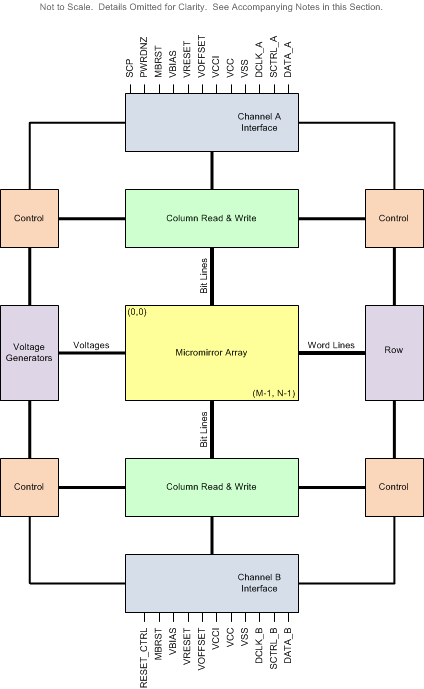
6.2
Functional Block Diagram
For pin details on Channels A, B, C, and D, refer to
Section 4
and the LVDS Interface section of
Section 5.8
. RESET_CTRL is used in applications when an external reset signal is required.