JAJSQ77 april   2023 DLP670RE

PRODUCTION DATA  

  1.   1
  2. 特長
  3. アプリケーション
  4. 説明
  5. Revision History
  6. Pin Configuration and Functions
  7. Specifications
    1. 6.1  Absolute Maximum Ratings
    2. 6.2  Storage Conditions
    3. 6.3  ESD Ratings
    4. 6.4  Recommended Operating Conditions
    5. 6.5  Thermal Information
    6. 6.6  Electrical Characteristics
    7. 6.7  Timing Requirements
    8. 6.8  System Mounting Interface Loads
    9. 6.9  Micromirror Array Physical Characteristics
    10. 6.10 Micromirror Array Optical Characteristics
    11. 6.11 Window Characteristics
    12. 6.12 Chipset Component Usage Specification
  8. Detailed Description
    1. 7.1 Overview
    2. 7.2 Functional Block Diagram
    3. 7.3 Feature Description
      1. 7.3.1 Power Interface
      2. 7.3.2 Timing
    4. 7.4 Device Functional Modes
    5. 7.5 Optical Interface and System Image Quality Considerations
      1. 7.5.1 Numerical Aperture and Stray Light Control
      2. 7.5.2 Pupil Match
      3. 7.5.3 Illumination Overfill
    6. 7.6 Micromirror Array Temperature Calculation
    7. 7.7 Micromirror Landed-On or Landed-Off Duty Cycle
      1. 7.7.1 Definition of Micromirror Landed-On or Landed-Off Duty Cycle
      2. 7.7.2 Landed Duty Cycle and Useful Life of the DMD
      3. 7.7.3 Landed Duty Cycle and Operational DMD Temperature
      4. 7.7.4 Estimating the Long-Term Average Landed Duty Cycle of a Product or Application
  9. Application and Implementation
    1. 8.1 Application Information
    2. 8.2 Typical Application
      1. 8.2.1 Design Requirements
      2. 8.2.2 Detailed Design Procedure
  10. Power Supply Requirements
    1. 9.1 DMD Power Supply Requirements
    2. 9.2 DMD Power Supply Power-Up Procedure
    3. 9.3 DMD Power Supply Power-Down Procedure
  11. 10Device Documentation Support
    1. 10.1 サード・パーティ製品に関する免責事項
    2. 10.2 Device Support
      1. 10.2.1 Device Nomenclature
      2. 10.2.2 Device Markings
    3. 10.3 Documentation Support
      1. 10.3.1 Related Documentation
    4. 10.4 Receiving Notification of Documentation Updates
    5. 10.5 サポート・リソース
    6. 10.6 Trademarks
    7. 10.7 静電気放電に関する注意事項
    8. 10.8 用語集
  12. 11Mechanical, Packaging, and Orderable Information

パッケージ・オプション

メカニカル・データ(パッケージ|ピン)
サーマルパッド・メカニカル・データ
発注情報

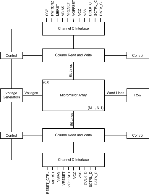
Functional Block Diagram

The main LVDS lines going to the DMD are connected via channel A and B. However, the LVDS lines come from channel C and D off the DLPC4430. Refer to the DLPC4430 Display Controller Data Sheet for more information.
GUID-61EBF960-FAFF-405E-93BB-34A09E8C0B2F-low.gif
For pin details on Channels A, B, C, and D, refer to Section 5 and LVDS Interface section of Timing Requirements.