JAJSIM5A November 2020 – June 2022 DLP670S
PRODUCTION DATA
- 1 特長
- 2 アプリケーション
- 3 概要
- 4 Revision History
- 5 Pin Configuration and Functions
-
6 Specifications
- 6.1 Absolute Maximum Ratings
- 6.2 Storage Conditions
- 6.3 ESD Ratings
- 6.4 Recommended Operating Conditions
- 6.5 Thermal Information
- 6.6 Electrical Characteristics
- 6.7 Capacitance at Recommended Operating Conditions
- 6.8 Timing Requirements
- 6.9 Typical Characteristics
- 6.10 System Mounting Interface Loads
- 6.11 Micromirror Array Physical Characteristics
- 6.12 Micromirror Array Optical Characteristics
- 6.13 Window Characteristics
- 6.14 Chipset Component Usage Specification
- 7 Detailed Description
- 8 Application and Implementation
- 9 Power Supply Recommendations
- 10Layout
- 11Device and Documentation Support
- 12Mechanical, Packaging, and Orderable Information
7.6 Micromirror Array Temperature Calculation
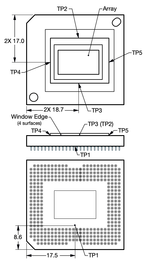
 Figure 7-1 DMD Thermal Test Points
Micromirror array temperature can be computed analytically from measurement points on the outside of the package, the package thermal resistance, the electrical power, and the illumination heat load. The relationship between micromirror array temperature and the reference ceramic temperature is provided by the following equations:
where
- TARRAY = Computed array temperature (°C)
- TCERAMIC = Measured ceramic temperature (°C) (measured at TP1 location)
- RARRAY-TO-CERAMIC = Thermal resistance of package specified in Thermal Information from array to ceramic TP1 (°C/Watt)
- QARRAY = Total DMD power on the array (W) (electrical + absorbed)
- QELECTRICAL = Nominal electrical power (W)
- QILLUMINATION = Illumination power absorbed (W)
The electrical power dissipation of the DMD is variable and depends on the voltages, data rates, and operating frequencies. A nominal electrical power dissipation to use when calculating array temperature is 3.32 W. The absorbed power from the illumination source is variable and depends on the operating state of the micromirrors and the intensity of the light source. The factors used in determining the illumination power absorbed is shown in each of the examples below. Examples are included where the optical power has been determined by measuring the illumination power density, total illumination power, and screen lumens. The examples assume illumination distribution is 83.7% on the active array and 16.3% on the area outside the array.