JAJSN06B September   2021  – March 2024 DLP780NE

PRODUCTION DATA  

  1.   1
  2. 特長
  3. アプリケーション
  4. 概要
  5. Pin Configuration and Functions
  6. Specifications
    1. 5.1  Absolute Maximum Ratings
    2. 5.2  Storage Conditions
    3. 5.3  ESD Ratings
    4. 5.4  Recommended Operating Conditions
    5.     11
    6. 5.5  Thermal Information
    7. 5.6  Electrical Characteristics
    8. 5.7  Timing Requirements
    9.     15
    10. 5.8  System Mounting Interface Loads
    11.     17
    12. 5.9  Micromirror Array Physical Characteristics
    13.     19
    14. 5.10 Micromirror Array Optical Characteristics
    15.     21
    16. 5.11 Window Characteristics
    17. 5.12 Chipset Component Usage Specification
  7. Detailed Description
    1. 6.1 Overview
    2. 6.2 Functional Block Diagram
    3. 6.3 Feature Description
      1. 6.3.1 Power Interface
      2. 6.3.2 Timing
    4. 6.4 Device Functional Modes
    5. 6.5 Optical Interface and System Image Quality Considerations
      1. 6.5.1 Numerical Aperture and Stray Light Control
      2. 6.5.2 Pupil Match
      3. 6.5.3 Illumination Overfill
    6. 6.6 Micromirror Array Temperature Calculation
    7. 6.7 Micromirror Power Density Calculation
    8. 6.8 Window Aperture Illumination Overfill Calculation
    9. 6.9 Micromirror Landed-On/Landed-Off Duty Cycle
      1. 6.9.1 Definition of Micromirror Landed-On/Landed-Off Duty Cycle
      2. 6.9.2 Landed Duty Cycle and Useful Life of the DMD
      3. 6.9.3 Landed Duty Cycle and Operational DMD Temperature
      4. 6.9.4 Estimating the Long-Term Average Landed Duty Cycle of a Product or Application
  8. Application and Implementation
    1. 7.1 Application Information
    2. 7.2 Typical Application
      1. 7.2.1 Design Requirements
      2. 7.2.2 Detailed Design Procedure
      3. 7.2.3 Application Curves
    3. 7.3 Temperature Sensor Diode
  9. Power Supply Recommendations
    1. 8.1 DMD Power Supply Requirements
    2. 8.2 DMD Power Supply Power-Up Procedure
    3. 8.3 DMD Power Supply Power-Down Procedure
  10. Layout
    1. 9.1 Layout Guidelines
    2. 9.2 Layout Example
      1. 9.2.1 Layers
      2. 9.2.2 Impedance Requirements
      3. 9.2.3 Trace Width, Spacing
        1. 9.2.3.1 Voltage Signals
  11. 10Device and Documentation Support
    1. 10.1 サード・パーティ製品に関する免責事項
    2. 10.2 Device Support
      1. 10.2.1 Device Nomenclature
    3. 10.3 Device Markings
    4. 10.4 Documentation Support
      1. 10.4.1 Related Documentation
    5. 10.5 ドキュメントの更新通知を受け取る方法
    6. 10.6 サポート・リソース
    7. 10.7 Trademarks
    8. 10.8 静電気放電に関する注意事項
    9. 10.9 用語集
  12. 11Revision History
  13. 12Mechanical, Packaging, and Orderable Information
パッケージ・オプション

メカニカル・データ(パッケージ|ピン)
サーマルパッド・メカニカル・データ
発注情報

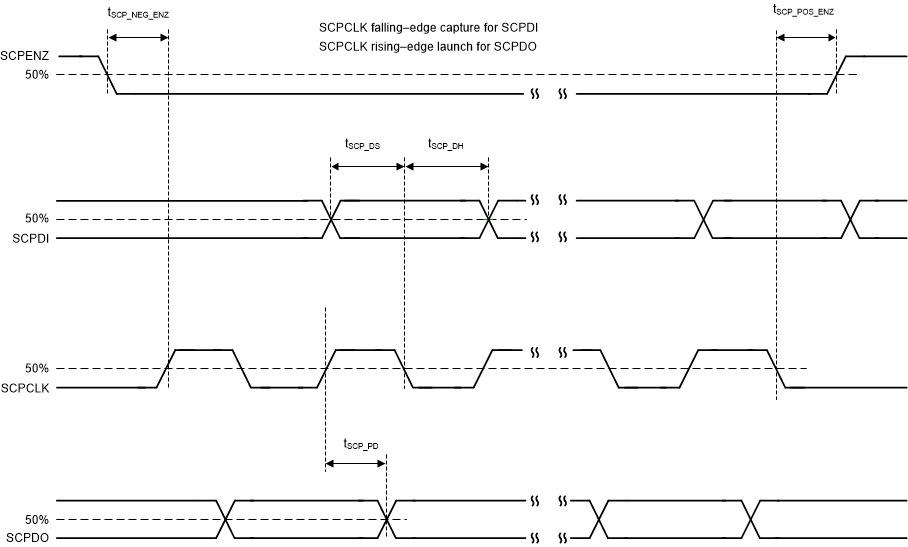
GUID-CBF8BEE5-467F-4921-BA83-B3A07CA654E6-low.gif Figure 5-3 SCP Timing Parameters
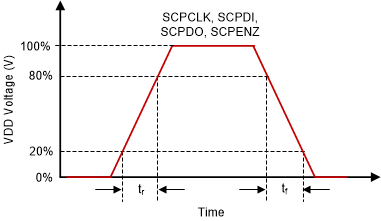
GUID-CCF5F336-2840-4075-9E88-353F42A002A8-low.gif Figure 5-4 SCP Rise and Fall Times
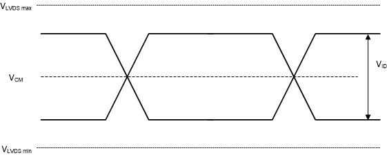
GUID-3C14D8F4-FBA3-4BD7-8C6D-A57A8638C3EA-low.gif Figure 5-5 LVDS Waveform Parameters
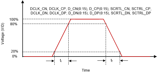
GUID-911C216A-4C8F-4724-9A6D-36176F9468EE-low.gif Figure 5-6 LVDS Rise and Fall Times
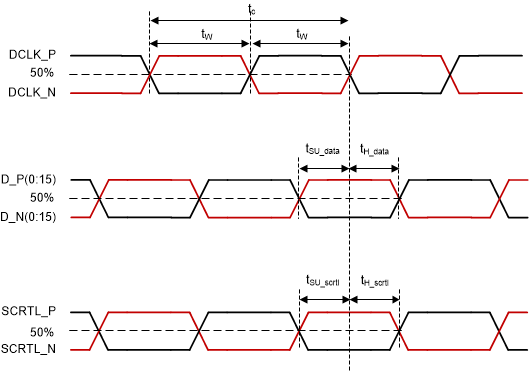
GUID-0389B9DD-0A18-4464-9BE6-FA2FB980846D-low.gif Figure 5-7 LVDS Timing Parameters
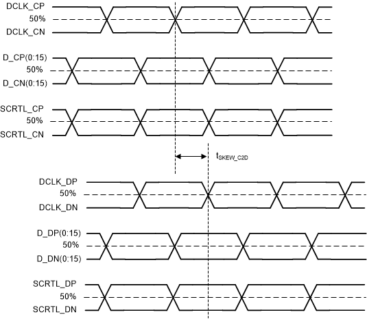
GUID-1A80764E-D13C-481D-9825-E96DBC3AE040-low.gif Figure 5-8 LVDS Skew Parameters