JAJSFJ1 May 2018 DLPA4000
PRODUCTION DATA.
- 1 特長
- 2 アプリケーション
- 3 概要
- 4 改訂履歴
- 5 概要(続き)
- 6 Pin Configuration and Functions
- 7 Specifications
-
8 Detailed Description
- 8.1 Overview
- 8.2 Functional Block Description
- 8.3
Feature Description
- 8.3.1 Supply and Monitoring
- 8.3.2 Illumination
- 8.3.3 External Power MOSFET Selection
- 8.3.4 DMD Supplies
- 8.3.5 Buck Converters
- 8.3.6 Auxiliary LDOs
- 8.3.7 Measurement System
- 8.4 Device Functional Modes
- 8.5 Programming
- 8.6 Register Maps
- 9 Application and Implementation
- 10Power Supply Recommendations
- 11Layout
- 12デバイスおよびドキュメントのサポート
- 13メカニカル、パッケージ、および注文情報
8.3.2.3 Illumination Driver A
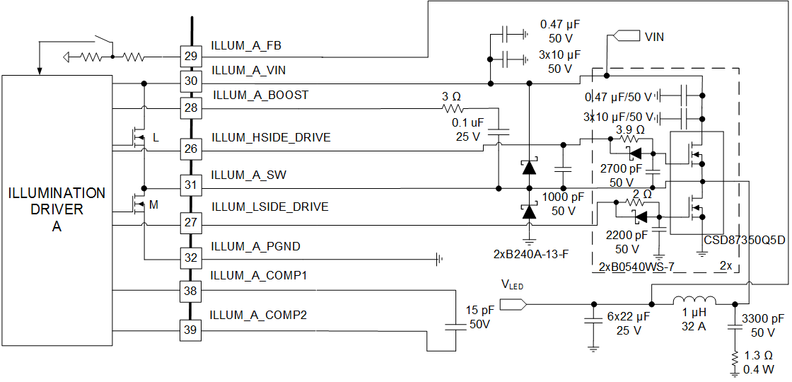
The illumination driver of the DLPA4000 comprises a buck controller for driving two external low-ohmic N-channel MOSFETs Figure 6). The application note Understanding Buck Power Stages in Switchmode Power Supplies (SLVA057) explains buck converter operation theory. Proper operation requires careful selection of the external components, especially the inductor LOUT and the output capacitor COUT. For best efficiency and ripple performance, choose an inductor and capacitor with low equivalent series resistance (ESR).
 Figure 6. Typical Illumination Driver Configuration
 Several factors determine the component selection of the buck converter, including input voltage (VIN), desired output voltage (VLED) and the allowed output current ripple. The first step of the configuration is to select the inductor LOUT.
Select the value of the inductance of a buck power stage so that the peak-to-peak ripple current flowing in the inductor remains within a certain range. Here, the target is set to have an inductor current ripple, kI_RIPPLE, less than 0.174 (17.4%). The minimum inductor value can be calculated given the input and output voltage, output current, switching frequency of the buck converter (ƒSWITCH= 600 kHz), and inductor ripple of 0.174 (17.4%):

Example: VIN= 19.5 V, VOUT= 4.3 V, IOUT= 32 A results in an inductor value of LOUT= 1µH
Determine the output capacitor, COUT after selecting the inductor. Calculate the value considering that the frequency compensation of the illumination loop is designed for an LC-tank resonance frequency of 13.8 kHz:

Example: COUT= 132 µF given that LOUT= 1 µH. A practical value is 6 × 22 µF. Here, a parallel connection of two capacitors is chosen to lower the ESR even further.
The selected inductor and capacitor determine the output voltage ripple. The resulting output voltage ripple VLED_RIPPLE is a function of the inductor ripple kI_RIPPLE, output current IOUT, switching frequency ƒSWITCH and the capacitor value COUT:

Example: KI_RIPPLE= 0.174, IOUT= 32 A, ƒSWITCH= 600 kHz and COUT= 6 x 22 µF results with an appropriately small level of 8.8 mVpp.
It is strongly advised to keep the capacitance value low. The larger the capacitor value the more energy is stored. When the LED voltage falls, stored energy must dissipate. Current discharges when stored energy dissipates. Use Equation 4 to calculate the theoretical peak reverse current caused by a large voltage drop.

where
- V1 is the starting VLED
- V2 is the ending VLED
- I1 is the LED current