JAJSFJ1 May   2018 DLPA4000

PRODUCTION DATA.  

  1. 特長
  2. アプリケーション
  3. 概要
    1.     Device Images
      1.      システム・ブロック図
  4. 改訂履歴
  5. 概要(続き)
  6. Pin Configuration and Functions
    1.     Pin Functions
  7. Specifications
    1. 7.1 Absolute Maximum Ratings
    2. 7.2 ESD Ratings
    3. 7.3 Recommended Operating Conditions
    4. 7.4 Thermal Information
    5. 7.5 Electrical Characteristics
    6. 7.6 SPI Timing Parameters
  8. Detailed Description
    1. 8.1 Overview
    2. 8.2 Functional Block Description
    3. 8.3 Feature Description
      1. 8.3.1 Supply and Monitoring
        1. 8.3.1.1 Supply
        2. 8.3.1.2 Monitoring
          1. 8.3.1.2.1 Block Faults
          2. 8.3.1.2.2 Low Battery and UVLO
          3. 8.3.1.2.3 Thermal Protection
      2. 8.3.2 Illumination
        1. 8.3.2.1 Programmable Gain Block
        2. 8.3.2.2 LDO Illumination
        3. 8.3.2.3 Illumination Driver A
        4. 8.3.2.4 External MOSFETs
          1. 8.3.2.4.1 Gate series resistor (RG)
          2. 8.3.2.4.2 Gate series diode (DG)
          3. 8.3.2.4.3 Gate parallel capacitance (CG)
        5. 8.3.2.5 RGB Strobe Decoder
          1. 8.3.2.5.1 Break Before Make (BBM)
          2. 8.3.2.5.2 Openloop Voltage
          3. 8.3.2.5.3 Transient Current Limit
        6. 8.3.2.6 Illumination Monitoring
          1. 8.3.2.6.1 Power Good
          2. 8.3.2.6.2 RatioMetric Overvoltage Protection
      3. 8.3.3 External Power MOSFET Selection
        1. 8.3.3.1 Threshold Voltage
        2. 8.3.3.2 Gate Charge and Gate Timing
        3. 8.3.3.3 On-resistance RDS(on)
      4. 8.3.4 DMD Supplies
        1. 8.3.4.1 LDO DMD
        2. 8.3.4.2 DMD HV Regulator
        3. 8.3.4.3 DMD/DLPC Buck Converters
        4. 8.3.4.4 DMD Monitoring
          1. 8.3.4.4.1 Power Good
          2. 8.3.4.4.2 Overvoltage Fault
      5. 8.3.5 Buck Converters
        1. 8.3.5.1 LDO Bucks
        2. 8.3.5.2 General Purpose Buck Converters
        3. 8.3.5.3 Buck Converter Monitoring
          1. 8.3.5.3.1 Power Good
          2. 8.3.5.3.2 Overvoltage Fault
      6. 8.3.6 Auxiliary LDOs
      7. 8.3.7 Measurement System
    4. 8.4 Device Functional Modes
    5. 8.5 Programming
      1. 8.5.1 SPI
      2. 8.5.2 Interrupt
      3. 8.5.3 Fast-Shutdown in Case of Fault
      4. 8.5.4 Protected Registers
      5. 8.5.5 Writing to EEPROM
    6. 8.6 Register Maps
  9. Application and Implementation
    1. 9.1 Application Information
    2. 9.2 Typical Application
      1. 9.2.1 Design Requirements
      2. 9.2.2 Detailed Design Procedure
        1. 9.2.2.1 Component Selection for General-Purpose Buck Converters
    3. 9.3 System Example With DLPA4000 Internal Block Diagram
  10. 10Power Supply Recommendations
    1. 10.1 Power-Up and Power-Down Timing
  11. 11Layout
    1. 11.1 Layout Guidelines
      1. 11.1.1 LED Driver
        1. 11.1.1.1 PowerBlock Gate Control Isolation
        2. 11.1.1.2 VIN to PowerBlocks
        3. 11.1.1.3 Return Current from LEDs and RSense
        4. 11.1.1.4 RC Snubber
        5. 11.1.1.5 Capacitor Choice
      2. 11.1.2 General Purpose Buck 2
      3. 11.1.3 SPI Connections
      4. 11.1.4 RLIM Routing
      5. 11.1.5 LED Connection
    2. 11.2 Layout Example
    3. 11.3 Thermal Considerations
  12. 12デバイスおよびドキュメントのサポート
    1. 12.1 デバイス・サポート
      1. 12.1.1 デバイスの項目表記
    2. 12.2 ドキュメントの更新通知を受け取る方法
    3. 12.3 コミュニティ・リソース
    4. 12.4 商標
    5. 12.5 静電気放電に関する注意事項
    6. 12.6 Glossary
  13. 13メカニカル、パッケージ、および注文情報
    1. 13.1 Package Option Addendum
      1. 13.1.1 Packaging Information

パッケージ・オプション

メカニカル・データ(パッケージ|ピン)
サーマルパッド・メカニカル・データ
発注情報

RatioMetric Overvoltage Protection

The DLPA4000 device protects the illumination driver LED outputs against open circuit use. When no LED is connected and the device receives a signal to set the LED current to a specific level, the LED voltage (ILLUM_A_FB) quickly rises and potentially saturates to VIN. The device triggers OVP protection circuit when VLED crosses the specified threshold to prevent this dangerous situation. The OVP protection fault disables the DLPA4000 device.

The device triggers a fault when the supply voltage (VINA) falls too low. A comparator senses both the LED voltage and the VINA supply voltage The fraction of the VINA is connected to the minus input of the comparator while the fraction of the VLED voltage is connected to the plus input. The OVP fault occurs when the plus input rises above the minus input. Set the fraction of the VINA between 1 V and 4 V to ensure proper operation of the comparator.
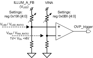
DLPA4000 OVP_Ratio-Metric.gifFigure 12. Ratio Metric OVP

Use register 0x19h bits [4:0] to set the fraction of the ILLUM_A_FB voltage. Use register 0x0Bh bits [4:0] to set the fraction of the VINA voltage. In general the device issues an OVP fault when either Equation 6 or Equation 6 occurs.

Equation 6. DLPA4000 q_vledovervledratio_dlps132.gif
Equation 7. DLPA4000 q_vled_dlps132.gif

Because the OVP level is ratio-metric it can be set to a fixed fraction of VINA.

For example: to maintain a VLED level below 85% of VINA, use these settings:

reg 0x19h [4:0] = 01h (4.98)

reg 0x0Bh [4:0] = 07h (5.85)

Additionally for VIN_RATIO = 5.85 the VIN– input voltage for the comparator is between 1 V and 3.4 V for a supply voltage between 6 V and 20 V.