JAJSFJ1 May   2018 DLPA4000

PRODUCTION DATA.  

  1. 特長
  2. アプリケーション
  3. 概要
    1.     Device Images
      1.      システム・ブロック図
  4. 改訂履歴
  5. 概要(続き)
  6. Pin Configuration and Functions
    1.     Pin Functions
  7. Specifications
    1. 7.1 Absolute Maximum Ratings
    2. 7.2 ESD Ratings
    3. 7.3 Recommended Operating Conditions
    4. 7.4 Thermal Information
    5. 7.5 Electrical Characteristics
    6. 7.6 SPI Timing Parameters
  8. Detailed Description
    1. 8.1 Overview
    2. 8.2 Functional Block Description
    3. 8.3 Feature Description
      1. 8.3.1 Supply and Monitoring
        1. 8.3.1.1 Supply
        2. 8.3.1.2 Monitoring
          1. 8.3.1.2.1 Block Faults
          2. 8.3.1.2.2 Low Battery and UVLO
          3. 8.3.1.2.3 Thermal Protection
      2. 8.3.2 Illumination
        1. 8.3.2.1 Programmable Gain Block
        2. 8.3.2.2 LDO Illumination
        3. 8.3.2.3 Illumination Driver A
        4. 8.3.2.4 External MOSFETs
          1. 8.3.2.4.1 Gate series resistor (RG)
          2. 8.3.2.4.2 Gate series diode (DG)
          3. 8.3.2.4.3 Gate parallel capacitance (CG)
        5. 8.3.2.5 RGB Strobe Decoder
          1. 8.3.2.5.1 Break Before Make (BBM)
          2. 8.3.2.5.2 Openloop Voltage
          3. 8.3.2.5.3 Transient Current Limit
        6. 8.3.2.6 Illumination Monitoring
          1. 8.3.2.6.1 Power Good
          2. 8.3.2.6.2 RatioMetric Overvoltage Protection
      3. 8.3.3 External Power MOSFET Selection
        1. 8.3.3.1 Threshold Voltage
        2. 8.3.3.2 Gate Charge and Gate Timing
        3. 8.3.3.3 On-resistance RDS(on)
      4. 8.3.4 DMD Supplies
        1. 8.3.4.1 LDO DMD
        2. 8.3.4.2 DMD HV Regulator
        3. 8.3.4.3 DMD/DLPC Buck Converters
        4. 8.3.4.4 DMD Monitoring
          1. 8.3.4.4.1 Power Good
          2. 8.3.4.4.2 Overvoltage Fault
      5. 8.3.5 Buck Converters
        1. 8.3.5.1 LDO Bucks
        2. 8.3.5.2 General Purpose Buck Converters
        3. 8.3.5.3 Buck Converter Monitoring
          1. 8.3.5.3.1 Power Good
          2. 8.3.5.3.2 Overvoltage Fault
      6. 8.3.6 Auxiliary LDOs
      7. 8.3.7 Measurement System
    4. 8.4 Device Functional Modes
    5. 8.5 Programming
      1. 8.5.1 SPI
      2. 8.5.2 Interrupt
      3. 8.5.3 Fast-Shutdown in Case of Fault
      4. 8.5.4 Protected Registers
      5. 8.5.5 Writing to EEPROM
    6. 8.6 Register Maps
  9. Application and Implementation
    1. 9.1 Application Information
    2. 9.2 Typical Application
      1. 9.2.1 Design Requirements
      2. 9.2.2 Detailed Design Procedure
        1. 9.2.2.1 Component Selection for General-Purpose Buck Converters
    3. 9.3 System Example With DLPA4000 Internal Block Diagram
  10. 10Power Supply Recommendations
    1. 10.1 Power-Up and Power-Down Timing
  11. 11Layout
    1. 11.1 Layout Guidelines
      1. 11.1.1 LED Driver
        1. 11.1.1.1 PowerBlock Gate Control Isolation
        2. 11.1.1.2 VIN to PowerBlocks
        3. 11.1.1.3 Return Current from LEDs and RSense
        4. 11.1.1.4 RC Snubber
        5. 11.1.1.5 Capacitor Choice
      2. 11.1.2 General Purpose Buck 2
      3. 11.1.3 SPI Connections
      4. 11.1.4 RLIM Routing
      5. 11.1.5 LED Connection
    2. 11.2 Layout Example
    3. 11.3 Thermal Considerations
  12. 12デバイスおよびドキュメントのサポート
    1. 12.1 デバイス・サポート
      1. 12.1.1 デバイスの項目表記
    2. 12.2 ドキュメントの更新通知を受け取る方法
    3. 12.3 コミュニティ・リソース
    4. 12.4 商標
    5. 12.5 静電気放電に関する注意事項
    6. 12.6 Glossary
  13. 13メカニカル、パッケージ、および注文情報
    1. 13.1 Package Option Addendum
      1. 13.1.1 Packaging Information

パッケージ・オプション

メカニカル・データ(パッケージ|ピン)
サーマルパッド・メカニカル・データ
発注情報

DMD HV Regulator

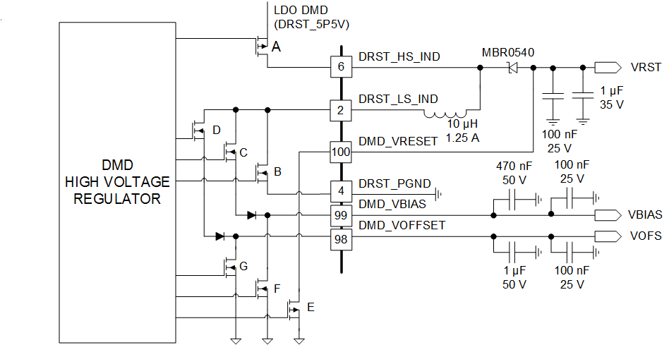
The DMD HV regulator generates three high voltage supplies: DMD_VRESET, DMD_VBIAS, and DMD_VOFFSET (see Figure 14). The DMD HV regulator uses a switching regulator (switch A through switch D), when the inductor shares time between all three supplies. The inductor charges to the current limit threshold and then discharged into one of the three supplies. The regulator distributes available charge time between those supplies that require a charge and when not all supplies require a charge.
DLPA4000 DLPA4000_HV_Regulator.gifFigure 14. DMD High Voltage Regulator